|
| |
• High-performance static CMOS technology– 100 MHz (10-ns cycle time)– 60 MHz (16.67-ns cycle time)– Low-power (1.8-V core, 3.3-V I/O) design
|
• JTAG boundary scan support– IEEE Standard 1149.1-1990 Standard Test Access Port and Boundary Scan Architecture
|
• High-performance 32-bit CPU (TMS320C28x)– 16 × 16 and 32 × 32 MAC operations– 16 × 16 dual MAC– Harvard bus architecture– Atomic operations– Fast interrupt response and processing– Unified memory programming model– Code-efficient (in C/C++ and Assembly)
|
• On-chip memory– F2809: 128K × 16 flash, 18K × 16 SARAM F2808: 64K × 16 flash, 18K × 16 SARAM F2806: 32K × 16 flash, 10K × 16 SARAM
F2802: 32K × 16 flash, 6K × 16 SARAM F2801: 16K × 16 flash, 6K × 16 SARAM F2801x: 16K × 16 flash, 6K × 16 SARAM– 1K × 16 OTP ROM (flash devices only)– C2802: 32K × 16 ROM, 6K × 16 SARAM C2801: 16K × 16 ROM, 6K × 16 SARAM |
| • Boot ROM (4K × 16)– With software boot modes (via SCI, SPI, CAN,I2C, and parallel I/O)– Standard math tables |
| • Clock and system control– On-chip oscillator– Watchdog timer module |
| • Any GPIO A pin can be connected to one of the three external core interrupts |
| • Peripheral Interrupt Expansion (PIE) block that supports all 43 peripheral interrupts |
| • Endianness: Little endian |
| • 128-bit security key/lock– Protects flash/OTP/L0/L1 blocks– Prevents firmware reverse-engineering |
| |
| CATALOG |
| TMS320F2809PZA COUNTRY OF ORIGIN |
TMS320F2809PZA PARAMETRIC INFO
|
TMS320F2809PZA PACKAGE INFO
|
TMS320F2809PZA MANUFACTURING INFO
|
TMS320F2809PZA PACKAGING INFO
|
TMS320F2809PZA EACD MODELS
|
| TMS320F2809PZA APPLICATIONS |
|
| COUNTRY OF ORIGIN |
| Taiwan (Province of China) |
| Philippines |
| |
PARAMETRIC INFO
|
| Data Bus Width (bit) |
32 |
| Family Name |
TMS320 |
| Instruction Set Architecture |
Harvard |
| Numeric and Arithmetic Format |
Floating-Point |
| Program Memory Size |
256KB |
| Program Memory Type |
Flash |
| RAM Size |
36KB |
| Maximum Speed (MHz) |
100 |
| Device Input Clock Speed (MHz) |
100 |
| Programmability |
Yes |
| Interface Type |
CAN/I2C/SPI/UART |
| Number of Programmable I/Os |
35 |
| Minimum Operating Supply Voltage (V) |
1.71|3.14 |
| Typical Operating Supply Voltage (V) |
1.8|3.3 |
| Maximum Operating Supply Voltage (V) |
1.89|3.47 |
| Minimum Operating Temperature (°C) |
-40 |
| Device Core |
C28x |
| Number of ADCs |
Single |
| ADC Channels |
16 |
| ADC Resolution (bit) |
12 |
| CAN |
2 |
| I2S |
0 |
| SPI |
4 |
| UART |
2 |
| USART |
0 |
| Ethernet |
0 |
| I2C |
1 |
| USB |
0 |
| Core Architecture |
C28x |
| Maximum Operating Temperature (°C) |
85 |
| Temperature Flag |
Opr |
| Operating Supply Voltage (V) |
1.8|3.3 |
|
|
PACKAGE INFO
|
| Supplier Package |
LQFP |
| Basic Package Type |
Lead-Frame SMT |
| Pin Count |
100 |
| Lead Shape |
Gull-wing |
| PCB |
100 |
| Tab |
N/R |
| Pin Pitch (mm) |
0.5 |
| Package Length (mm) |
14.2(Max) |
| Package Width (mm) |
14.2(Max) |
| Package Height (mm) |
1.45(Max) |
| Package Diameter (mm) |
N/R |
| Package Overall Length (mm) |
16.2(Max) |
| Package Overall Width (mm) |
16.2(Max) |
| Package Overall Height (mm) |
1.6(Max) |
| Seated Plane Height (mm) |
1.6(Max) |
| Mounting |
Surface Mount |
| Package Weight (g) |
N/A |
| Package Material |
Plastic |
| Package Description |
Low Profile Quad Flat Package |
| Package Family Name |
QFP |
| Jedec |
MS-026 |
| Package Outline |
Link to Datasheet |
|
|
MANUFACTURING INFO
|
| MSL |
2 |
| Maximum Reflow Temperature (°C) |
260 |
| Reflow Solder Time (Sec) |
30 |
| Number of Reflow Cycle |
3 |
| Standard |
J-STD-020D |
| Reflow Temp. Source |
Link to Datasheet |
| Maximum Wave Temperature (°C) |
N/R |
| Wave Solder Time (Sec) |
N/R |
| Lead Finish(Plating) |
Au |
| Under Plating Material |
Pd over Ni |
| Terminal Base Material |
Cu Alloy |
|
|
PACKAGING INFO
|
| Packaging |
Tray |
| Quantity Of Packaging |
90 |
| Packaging Document |
Link to Datasheet |
|
|
ECAD MODELS
|
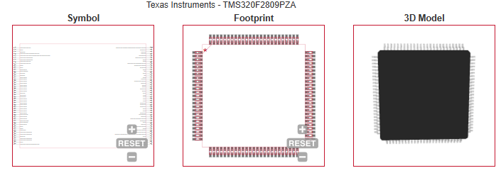
|
| APPLICATIONS |
| • Motor drive and control |
| • Digital power |
| |