|
|
| • High Efficiency Integrated Boost Converter (Over 90% Efficiency) |
• 2.2-W into an 8-Ω Load from a 3.6-V Supply
|
• 2.7-W into an 4-Ω Load from a 3.6-V Supply
|
• Operates from 1.8 V to 5.5 V
|
• Efficient Class-D Prolongs Battery Life
|
• Independent Shutdown for Boost Converter and Class-D Amplifier
|
• Differential Inputs Reduce RF Common Noise
|
• Built-In INPUT Low-Pass Filter Decreases RF and Out-of-Band Noise Sensitivity
|
• Synchronized Boost and Class-D Eliminates Beat Frequencies
|
|
| CATALOG |
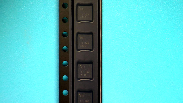
TPA2013D1RGPR COUNTRY OF ORIGIN
|
TPA2013D1RGPR PARAMETRIC INFO
|
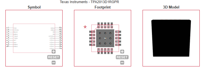
TPA2013D1RGPR PACKAGE INFO
|
TPA2013D1RGPR MANUFACTURING INFO
|
TPA2013D1RGPR PACKAGING INFO
|
TPA2013D1RGPR ECAD MODELS
|
| TPA2013D1RGPR APPLICATIONS |
|
COUNTRY OF ORIGIN
|
Malaysia
|
|
PARAMETRIC INFO
|
| Amplifier Type |
Class-D |
| Function |
Speaker |
| Input Signal Type |
Differential |
| Output Signal Type |
Differential |
| Output Type |
1-Channel Mono |
| Power Supply Type |
Dual |
| Minimum Dual Supply Voltage (V) |
1.8|3 |
| Typical Dual Supply Voltage (V) |
3|5 |
| Maximum Dual Supply Voltage (V) |
5.5 |
| Maximum Load Resistance (Ohm) |
8 |
| Maximum Output Current (mA) |
1700 |
| Typical Output Power (W) |
2.7 |
| Typical Output Power x Channels @ Load (W) |
2.7x1@4Ohm |
| Maximum Power Dissipation (mW) |
2500 |
| Typical Quiescent Current (mA) |
16.5@3.6V/4.3@5.5V |
| Maximum Quiescent Current (mA) |
23@3.6V/6@5.5V |
| Minimum CMRR (dB) |
75(Typ) |
| Total Harmonic Distortion Noise |
10%@8Ohm@2.2W|0.1%@8Ohm@1W |
| Typical Voltage Gain (dB) |
20 |
| Minimum Operating Temperature (°C) |
-40 |
| Maximum Operating Temperature (°C) |
85 |
| Minimum Storage Temperature (°C) |
-65 |
| Maximum Storage Temperature (°C) |
150 |
|
|
PACKAGE INFO
|
| Supplier Package |
VQFN EP |
| Basic Package Type |
Non-Lead-Frame SMT |
| Pin Count |
20 |
| Lead Shape |
No Lead |
| PCB |
20 |
| Tab |
N/R |
| Pin Pitch (mm) |
0.5 |
| Package Length (mm) |
4.15(Max) |
| Package Width (mm) |
4.15(Max) |
| Package Height (mm) |
0.95(Max) |
| Package Diameter (mm) |
N/R |
| Package Overall Length (mm) |
4.15(Max) |
| Package Overall Width (mm) |
4.15(Max) |
| Package Overall Height (mm) |
1(Max) |
| Seated Plane Height (mm) |
1(Max) |
| Mounting |
Surface Mount |
| Package Weight (g) |
N/A |
| Package Material |
Plastic |
| Package Description |
Very Thin Quad Flat No Lead Package, Exposed Pad |
| Package Family Name |
QFN |
| Package Outline |
Link to Datasheet |
|
|
MANUFACTURING INFO
|
| MSL |
3 |
| Maximum Reflow Temperature (°C) |
260 |
| Reflow Solder Time (Sec) |
30 |
| Number of Reflow Cycle |
3 |
| Standard |
J-STD-020D |
| Reflow Temp. Source |
Link to Datasheet |
| Maximum Wave Temperature (°C) |
N/R |
| Wave Solder Time (Sec) |
N/R |
| Lead Finish(Plating) |
Au |
| Under Plating Material |
Pd over Ni |
| Terminal Base Material |
Cu Alloy |
|
|
PACKAGING INFO
|
| Packaging Suffix |
R |
| Packaging |
Tape and Reel |
| Quantity Of Packaging |
3000 |
| Packaging Document |
Link to Datasheet |
|
|
| ECAD MODELS |
|
|
| APPLICATIONS |
| • Cell Phones |
| • PDA |
| • GPS |
| • Portable Electronics |
| |