 |
|
• IEC 61000-4-2 ESD Protection (Level 4)
– ±8-kV Contact Discharge
– ±15-kV Air-Gap Discharge |
| • 5.5-A Peak Pulse Current (8/20-µs Pulse) |
| • IO Capacitance: 1.5 pF (Typical)
|
| • Low Leakage Current: 1 nA (Maximum) |
| • Low Supply Current: 1 nA |
| • 0.9-V to 5.5-V Supply-Voltage Range |
| • Space-Saving DRL, DBV, DCK, DPK, and DRS
Package Options |
| • Alternate 2, 3, 6-Channel options Available:
TPD2E001, TPD3E001, TPD6E001
|
|
| CATALOG |
| TPD4E001DCKR COUNTRY OF ORIGIN |
| TPD4E001DCKR PARAMETRIC INFO |
| TPD4E001DCKR PACKAGE INFO |
| TPD4E001DCKR MANUFACTURING INFO |
| TPD4E001DCKR PACKAGING INFO |
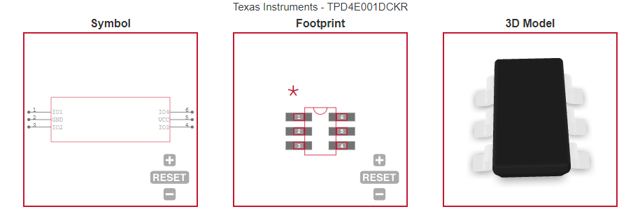
| TPD4E001DCKR ECAD MODELS |
| TPD4E001DCKR FUNCTIONAL BLOCK DIAGRAM |
| TPD4E001DCKR APPLICATIONS |
|
| COUNTRY OF ORIGIN |
| China |
| Thailand |
|
| PARAMETRIC INFO |
| Type |
Diode Array |
| Direction Type |
Uni-Directional |
| Maximum Working Voltage (V) |
5.5 |
| Configuration |
Quad |
| Capacitance Value (pF) |
1.5(Typ) |
| Maximum Clamping Voltage (V) |
105.5 |
| Maximum Leakage Current (uA) |
0.001 |
| Operating Junction Temperature (°C) |
150 |
| Number of Elements per Chip |
4 |
| Test Current (mA) |
10 |
| Peak Pulse Power Dissipation (W) |
100@8/20us |
| Maximum Peak Pulse Current (A) |
5.5@8/20us |
| Minimum Breakdown Voltage (V) |
11 |
| Minimum Operating Temperature (°C) |
-40 |
| Fail Safe Protection |
Yes |
| Maximum Operating Temperature (°C) |
85 |
| Minimum Storage Temperature (°C) |
-65 |
| Maximum Storage Temperature (°C) |
150 |
|
| |
| PACKAGE INFO |
| Supplier Package |
SC-70 |
| Basic Package Type |
Lead-Frame SMT |
| Pin Count |
6 |
| Lead Shape |
Gull-wing |
| PCB |
6 |
| Tab |
N/R |
| Pin Pitch (mm) |
0.65 |
| Package Length (mm) |
2.15(Max) |
| Package Width (mm) |
1.4(Max) |
| Package Height (mm) |
1(Max) |
| Package Diameter (mm) |
N/R |
| Package Overall Length (mm) |
2.15(Max) |
| Package Overall Width (mm) |
2.4(Max) |
| Package Overall Height (mm) |
1.1(Max) |
| Seated Plane Height (mm) |
1.1(Max) |
| Mounting |
Surface Mount |
| Package Weight (g) |
N/A |
| Package Material |
Plastic |
| Package Description |
Small Outline Transistor |
| Package Family Name |
SOT |
| Jedec |
MO-203AB |
| Package Outline |
Link to Datasheet |
|
| |
| MANUFACTURING INFO |
| MSL |
1 |
| Maximum Reflow Temperature (°C) |
260 |
| Reflow Solder Time (Sec) |
30 |
| Number of Reflow Cycle |
3 |
| Standard |
J-STD-020D |
| Reflow Temp. Source |
Link to Datasheet |
| Maximum Wave Temperature (°C) |
N/R |
| Wave Solder Time (Sec) |
N/R |
| Wave Temp. Source |
Link to Datasheet |
| Lead Finish(Plating) |
Au |
| Under Plating Material |
Pd over Ni |
| Terminal Base Material |
Cu Alloy |
| Number of Wave Cycles |
N/R |
|
| |
| PACKAGING INFO |
| Packaging Suffix |
R |
| Packaging |
Tape and Reel |
| Quantity Of Packaging |
3000 |
| Reel Diameter (in) |
7 |
| Tape Pitch (mm) |
4 |
| Tape Width (mm) |
8 |
| Component Orientation |
Q3 |
| Packaging Document |
Link to Datasheet |
|
| |
| ECAD MODELS |
 |
|
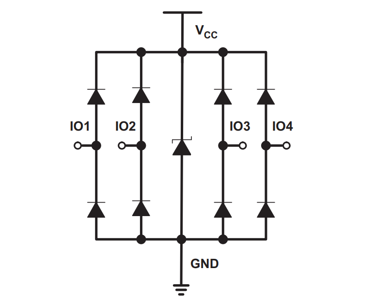
| FUNCTIONAL BLOCK DIAGRAM |
 |
|
| Applications |
| • USB 2.0 |
| • Ethernet |
| • FireWire™ Serial Bus
|
| • LVDS |
| • SVGA Video Connections
|
| • Glucose Meters |
|