|
|
• Integrated Single Channel Load Switch
|
• Ambient Operating Temperature:–40°C to +105°C– SOT23-6 (DBV): 2-A Maximum ContinuousCurrent 1– WSON (DRV): 3-A Maximum Continuous Current 1
|
• Input Voltage Range: 2.7 V to 18 V
|
| • Absolute Maximum Input Voltage: 20 V
|
| • On-Resistance (RON)– RON = 79 mΩ (typical) at VIN = 12 V |
| • Quiescent Current– 62 µA (typical) at VIN = 12 V |
| • Shutdown Current– 500 nA (typical) at VIN = 12 V |
| • Thermal Shutdown |
| • Undervoltage Lock-Out (UVLO) |
| • Adjustable Quick Output Discharge (QOD) |
| • Configurable Rise Time With CT Pin |
| • SOT23-6 Package– 2.9-mm × 2.8-mm, 0.95-mm Pitch 1.45-mm Height (DBV) |
• WSON Package– 2-mm × 2-mm, 0.65-mm Pitch 0.75-mm Height (DRV)
|
| • ESD Performance Tested per JESD 22– ±2-kV HBM and ±1-kV CDM |
| |
| CATALOG |
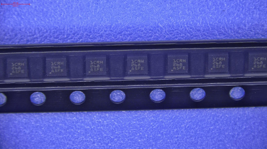
| TPS22810DRVR COUNTRY OF ORIGIN |
TPS22810DRVR PARAMETRIC INFO
|
TPS22810DRVR PACKAGE INFO
|
TPS22810DRVR MANUFACTURING INFO
|
TPS22810DRVR PACKAGING INFO
|
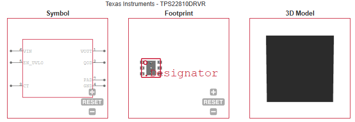
TPS22810DRVR EACD MODELS
|
| TPS22810DRVR APPLICATIONS |
|
| COUNTRY OF ORIGIN |
| Philippines |
| Thailand |
| China |
|
PARAMETRIC INFO
|
| type |
High Side |
| Number of Outputs |
1 |
| Maximum Input Voltage (V) |
18 |
| Minimum Output Current (A) |
3(Max) |
| Minimum Operating Temperature (°C) |
-40 |
| Minimum Input Voltage (V) |
2.7 |
| Maximum Operating Temperature (°C) |
105 |
| Switch On Resistance (Ohm) |
0.086 |
| Output Voltage Range (V) |
18(Max) |
| Operating Supply Voltage Range (V) |
2.7 to 18 |
| Minimum Storage Temperature (°C) |
-65 |
| Maximum Storage Temperature (°C) |
150 |
|
|
PACKAGE INFO
|
| Supplier packaging |
WSON EP |
| Basic package type |
Non-Lead-Frame SMT |
| Number of pins |
6 |
| Pin shape |
No Lead |
| PCB |
6 |
| ears |
N/R |
| Pin spacing (mm) |
0.65 |
| Package length (mm) |
2.1(Max) |
| Package width (mm) |
2.1(Max) |
| Package height (mm) |
0.75(Max) |
| Package diameter (mm) |
N/R |
| Package Overall Length (mm) |
2.1(Max) |
| Package Overall Width (mm) |
2.1(Max) |
| Package Overall Height (mm) |
0.8(Max) |
| Mounting surface height (mm) |
0.8(Max) |
| Install |
Surface Mount |
| Package weight (g) |
not applicable |
| Packaging materials |
Plastic |
| package instruction |
Very Very Thin Small Outline No Lead Package, Exposed Pad |
| Package series name |
SON |
| JEDEC |
not applicable |
|
|
MANUFACTURING INFO
|
| MSL |
1 |
| Maximum reflow temperature (°C) |
260 |
| Reflow soldering time (seconds) |
30 |
| Number of reflow cycles |
3 |
| Reflow temperature source |
Link to datasheet |
| Maximum wave soldering temperature (°C) |
N/R |
| Wave soldering time (seconds) |
N/R |
| Lead Finish(Plating) |
Au |
| Plating materials |
Pd over Ni |
| Terminal Base Material |
Cu Alloy |
|
|
PACKAGING INFO
|
| Packaging Suffix |
R |
| Package |
Tape and reel packaging |
| Packing quantity |
3000 |
| Reel Diameter (in) |
7.09 |
| Reel Width (mm) |
8.4 |
| Tape Pitch (mm) |
4 |
| Tape Width (mm) |
8 |
| Component Orientation |
Q2 |
| packaging type file |
Link to datasheet |
|
|
ECAD MODELS
|
|
|
| APPLICATIONS |
| • HD TV |
| • Industrial Systems |
| • Set Top Box |
| • Surveillance systems |
| |