|
|
• Input Voltage: Supports 2.5-V Rail and 3.3-V Rail
|
• VLDOIN Voltage Range: 1.1 V to 3.5 V
|
• Sink and Source Termination Regulator Includes Droop Compensation
|
| • Requires Minimum Output Capacitance of 20-μF(Typically 3 × 10-μF MLCCs) for Memory Termination Applications (DDR)
|
| • PGOOD to Monitor Output Regulation |
| • EN Input |
| • REFIN Input Allows for Flexible Input Tracking Either Directly or Through Resistor Divider |
| • Remote Sensing (VOSNS) |
| •±10-mA Buffered Reference (REFOUT) |
| • Built-in Soft Start, UVLO, and OCL |
| • Thermal Shutdown |
| • Supports DDR, DDR2, DDR3, DDR3L, LowPower DDR3, and DDR |
| • 10-Pin VSON Package With Thermal Pad |
|
| CATALOG |
| TPS51200DRCR COUNTRY OF ORIGIN |
TPS51200DRCR PARAMETRIC INFO
|
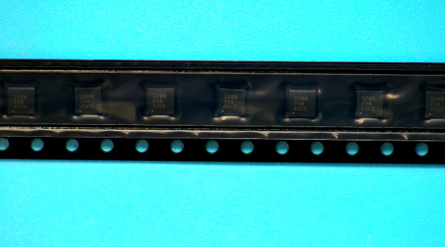
TPS51200DRCR PACKAGE INFO
|
TPS51200DRCR MANUFACTURING INFO
|
TPS51200DRCR PACKAGING INFO
|
TPS51200DRCR EACD MODELS
|
| TPS51200DRCR APPLICATIONS |
|
| COUNTRY OF ORIGIN |
| Malaysia |
| China |
| Philippines |
| Thailand |
|
PARAMETRIC INFO
|
| Category |
DDR Termination Regulator |
| Number of Outputs |
1 |
| Input Voltage (V) |
2.375 to 3.5 |
| Minimum Operating Temperature (°C) |
-40 |
| Maximum Operating Temperature (°C) |
85 |
| Minimum Operating Supply Voltage (V) |
2.375 |
| Maximum Operating Supply Voltage (V) |
3.5 |
| Maximum Supply Current (mA) |
1 |
| Output Current (A) |
3(Max) |
| Maximum Storage Temperature (°C) |
150 |
| Minimum Storage Temperature (°C) |
-55 |
|
|
PACKAGE INFO
|
| Supplier packaging |
VSON EP |
| Basic package type |
Non-Lead-Frame SMT |
| Number of pins |
10 |
| Pin shape |
No Lead |
| PCB |
10 |
| ears |
N/R |
| Pin spacing (mm) |
0.5 |
| Package length (mm) |
3.1(Max) |
| Package width (mm) |
3.1(Max) |
| Package height (mm) |
0.95(Max) |
| Package diameter (mm) |
N/R |
| Package Overall Length (mm) |
3.1(Max) |
| Package Overall Width (mm) |
3.1(Max) |
| Package Overall Height (mm) |
1(Max) |
| Mounting surface height (mm) |
1(Max) |
| Install |
Surface Mount |
| Package weight (g) |
not applicable |
| Packaging materials |
Plastic |
| package instruction |
Very Thin Small Outline No Lead, Exposed Pad |
| Package series name |
SON |
| JEDEC |
not applicable |
|
|
MANUFACTURING INFO
|
| MSL |
2 |
| Maximum reflow temperature (°C) |
260 |
| Reflow soldering time (seconds) |
30 |
| Number of reflow cycles |
3 |
| standard |
J-STD-020D |
| Reflow temperature source |
Link to datasheet |
| Maximum wave soldering temperature (°C) |
N/R |
| Wave soldering time (seconds) |
N/R |
| Lead Finish(Plating) |
Au |
| Plating materials |
Pd over Ni |
| Terminal Base Material |
Cu Alloy |
| Number of Wave Cycles |
N/R |
|
|
PACKAGING INFO
|
| Packaging Suffix |
R |
| Package |
Tape and reel packaging |
| Packing quantity |
3000 |
| Reel Diameter (in) |
13 |
| Reel Width (mm) |
12.4 |
| Tape Pitch (mm) |
8 |
| Tape Width (mm) |
12 |
| Component Orientation |
Q2 |
| packaging type file |
Link to datasheet |
|
|
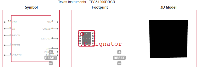
ECAD MODELS
|
|
|
APPLICATIONS
|
• Memory Termination Regulator for DDR, DDR2,DDR3, DDR3L, Low-Power DDR3 and DDR4
|
| • Notebooks, Desktops, and Servers |
| • Telecom and Datacom |
| • Base Stations |
| • LCD-TVs and PDP-TVs |
| • Copiers and Printers |
| • Set-Top Boxes |
| |