 |
|
| • 3.5-V to 60-V Input Voltage Range
|
| • 200-mΩ High-Side MOSFET |
| • High Efficiency at Light Loads With a PulseSkipping Eco-mode™
|
| • 138-μA Operating Quiescent Current |
| • 1.3-μA Shutdown Current |
| • 100-kHz to 2.5-MHz Switching Frequency• 100-kHz to 2.5-MHz Switching Frequency |
| • Synchronizes to External Clock
|
| • Adjustable Slow Start and Sequencing |
| • UV and OV Powergood Output |
| • Adjustable UVLO Voltage and Hysteresis |
| • 0.8-V Internal Voltage Reference
|
| • 10-Pin MSOP and 10-Pin 3-mm × 3-mm VSON
With PowerPAD™ Packages |
| • Create a Custom Design Using the TPS54260
With WEBENCH® Power Designer |
|
| CATALOG |
| TPS54260DGQR COUNTRY OF ORIGIN |
| TPS54260DGQR PARAMETRIC INFO |
| TPS54260DGQR PACKAGE INFO |
| TPS54260DGQR MANUFACTURING INFO |
| TPS54260DGQR PACKAGING INFO |
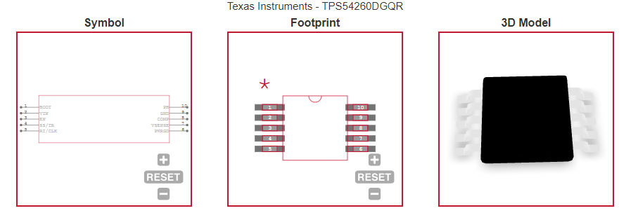
| TPS54260DGQR ECAD MODELS |
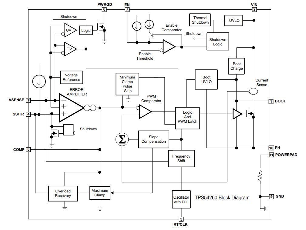
| TPS54260DGQR FUNCTIONAL BLOCK DIAGRAM |
| TPS54260DGQR APPLICATIONS |
|
| COUNTRY OF ORIGIN |
| China |
| Thailand |
|
| PARAMETRIC INFO |
| Type |
Synchronous Step Down |
| Number of Outputs |
1 |
| Minimum Input Voltage (V) |
3.5 |
| Maximum Input Voltage (V) |
60 |
| Output Voltage (V) |
0.8 to 58 |
| Maximum Output Current (A) |
2.5 |
| Minimum Operating Temperature (°C) |
-40 |
| Maximum Operating Temperature (°C) |
125 |
| Switching Frequency (kHz) |
2500 |
| Switching Regulator |
Yes |
| Operating Supply Voltage (V) |
3.5 to 60 |
| Output Type |
Adjustable |
| Tradename |
Eco-Mode™ |
| Typical Quiescent Current (uA) |
138 |
| Minimum Storage Temperature (°C) |
-65 |
| Maximum Storage Temperature (°C) |
150 |
| Typical Switch Current (A) |
6.1 |
|
| |
| PACKAGE INFO |
| Supplier Package |
HVSSOP EP |
| Basic Package Type |
Lead-Frame SMT |
| Pin Count |
10 |
| Lead Shape |
Gull-wing |
| PCB |
10 |
| Tab |
N/R |
| Pin Pitch (mm) |
0.5 |
| Package Length (mm) |
3.1(Max) |
| Package Width (mm) |
3.1(Max) |
| Package Height (mm) |
0.95(Max) |
| Package Diameter (mm) |
N/R |
| Package Overall Length (mm) |
3.1(Max) |
| Package Overall Width (mm) |
5.05(Max) |
| Package Overall Height (mm) |
1.1(Max) |
| Seated Plane Height (mm) |
1.1(Max) |
| Mounting |
Surface Mount |
| Package Weight (g) |
N/A |
| Package Material |
Plastic |
| Package Description |
Heat Sinked Very Thin Shrink Small Outline Package, Exposed Pad |
| Package Family Name |
SOP |
| Jedec |
MO-187BA-T |
| Package Outline |
Link to Datasheet |
|
| |
| MANUFACTURING INFO |
| MSL |
1 |
| Maximum Reflow Temperature (°C) |
260 |
| Reflow Solder Time (Sec) |
30 |
| Number of Reflow Cycle |
3 |
| Standard |
J-STD-020D |
| Reflow Temp. Source |
Link to Datasheet |
| Maximum Wave Temperature (°C) |
N/R |
| Wave Solder Time (Sec) |
N/R |
| Lead Finish(Plating) |
Au |
| Under Plating Material |
Pd over Ni|PdNiAg |
| Terminal Base Material |
Cu Alloy |
|
| |
| PACKAGING INFO |
| Packaging |
Tape and Reel |
| Quantity Of Packaging |
2500 |
|
| |
| ECAD MODELS |
 |
|
| FUNCTIONAL BLOCK DIAGRAM |
|
|
| APPLICATIONS |
| • 12-V, 24-V and 48-V Industrial and Commercial
Low-Power Systems |
| • GSM, GPRS Modules in Fleet Management, EMeters, and Security Systems |
|