|
|
• 1.8-V to 6-V Input Voltage Range
|
• Adjustable Output Voltage Range up to 28 V
|
• 400-mA (TPS61040) and 250-mA (TPS61041)Internal Switch Current
|
• Up to 1-MHz Switching Frequency
|
• 28-μA Typical No-Load Quiescent Current
|
• 1-μA Typical Shutdown Current
|
• Internal Soft Start
|
• Available in SOT23-5, TSOT23-5,and 2-mm × 2-mm × 0.8-mm WSON Packages
|
|
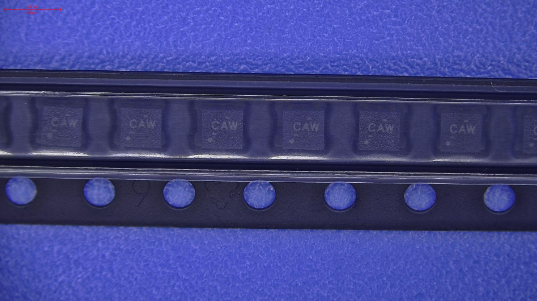
| CATALOG |
TPS61041DRVT Country of Origin
|
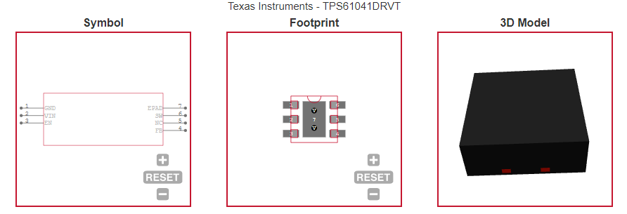
TPS61041DRVT Parametric Info
|
TPS61041DRVT Package Info
|
TPS61041DRVT Manufacturing Info
|
TPS61041DRVT Packaging Info
|
TPS61041DRVT ECAD Models
|
TPS61041DRVT Functional Block Diagram
|
TPS61041DRVT Applications
|
|
COUNTRY OF ORIGINV
|
Thailand
|
China
|
Malaysia
|
Philippines
|
|
PARAMETRIC INFO
|
| Type |
Step Up |
| Number of Outputs |
1 |
| Minimum Input Voltage (V) |
1.8 |
| Maximum Input Voltage (V) |
6 |
| Output Voltage (V) |
1.8 to 28 |
| Minimum Operating Temperature (°C) |
-40 |
| Maximum Operating Temperature (°C) |
85 |
| Regulation Condition Change In Load |
30mA |
| Regulation Condition Change In Line |
4.2V |
| Switching Frequency (kHz) |
1000 |
| Switching Regulator |
Yes |
| Operating Supply Voltage (V) |
1.8 to 6 |
| Output Type |
Adjustable |
| Load Regulation |
0.15%/mA(Typ) |
| Line Regulation |
0.05%/V(Typ) |
| Typical Quiescent Current (uA) |
28 |
| Minimum Storage Temperature (°C) |
-65 |
| Maximum Storage Temperature (°C) |
150 |
| Typical Switch Current (A) |
0.25 |
|
|
PACKAGE INFO
|
| Supplier Package |
WSON EP |
| Basic Package Type |
Non-Lead-Frame SMT |
| Pin Count |
6 |
| Lead Shape |
No Lead |
| PCB |
6 |
| Tab |
N/R |
| Pin Pitch (mm) |
0.65 |
| Package Length (mm) |
2.1(Max) |
| Package Width (mm) |
2.1(Max) |
| Package Height (mm) |
0.75(Max) |
| Package Diameter (mm) |
N/R |
| Package Overall Length (mm) |
2.1(Max) |
| Package Overall Width (mm) |
2.1(Max) |
| Package Overall Height (mm) |
0.8(Max) |
| Seated Plane Height (mm) |
0.8(Max) |
| Mounting |
Surface Mount |
| Package Weight (g) |
N/A |
| Package Material |
Plastic |
| Package Description |
Very Very Thin Small Outline No Lead Package, Exposed Pad |
| Package Family Name |
SON |
| Jedec |
N/A |
|
|
MANUFACTURING INFO
|
| MSL |
1 |
| Maximum Reflow Temperature (°C) |
260 |
| Reflow Solder Time (Sec) |
30 |
| Number of Reflow Cycle |
3 |
| Standard |
J-STD-020D |
| Reflow Temp. Source |
Link to Datasheet |
| Maximum Wave Temperature (°C) |
N/R |
| Wave Solder Time (Sec) |
N/R |
| Wave Temp. Source |
Link to Datasheet |
| Lead Finish(Plating) |
Au |
| Under Plating Material |
Pd over Ni |
| Terminal Base Material |
Cu Alloy |
| Number of Wave Cycles |
N/R |
|
|
PACKAGING INFO
|
| Packaging Suffix |
T |
| Packaging |
Tape and Reel |
| Quantity Of Packaging |
250 |
| Reel Diameter (in) |
7 |
| Reel Width (mm) |
8.4 |
| Tape Pitch (mm) |
4 |
| Tape Width (mm) |
8 |
| Component Orientation |
Q2 |
| Packaging Document |
Link to Datasheet |
|
|
ECAD MODELS
|
|
|
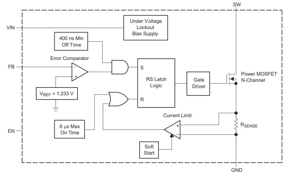
FUNCTIONAL BLOCK DIAGRAM
|
|
|
APPLICATIONS
|
• LCD Bias Supply
|
• White-LED Supply for LCD Backlights
|
• Digital Still Camera
|
• PDAs, Organizers, and Handheld PCs
|
• Cellular Phones
|
• Internet Audio Players
|
• Standard 3.3-V or 5-V to 12-V Conversion
|
|
|