|
| |
• DCS-Control™ Topology
|
• Input Voltage Range from 3 V to 17 V
|
• Up to 1-A Output Current
|
| • Adjustable Output Voltage From 0.9 V to 6 V |
| • Fixed Output Voltage Versions |
| • Seamless Power Save Mode Transition |
| • Typically 17-µA Quiescent Current |
| • Power Good Output |
| • 100% Duty Cycle Mode |
| • Short Circuit Protection |
| • Over Temperature Protection |
| • Pin to Pin Compatible With TPS62170 and TPS62125 |
| • Available in 3.00 mm x 3.00 mm 8-Pin VSSOP and 2.00 mm × 2.00 mm 8-Pin WSON Packages |
| • Create a Custom Design using the TPS62160 with the WEBENCH® Power Designer |
| |
| CATALOG |
| TPS62160DSGR COUNTRY OF ORIGIN |
TPS62160DSGR PARAMETRIC INFO
|
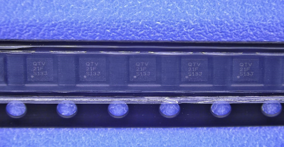
TPS62160DSGR PACKAGE INFO
|
TPS62160DSGR MANUFACTURING INFO
|
TPS62160DSGR PACKAGING INFO
|
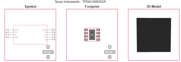
TPS62160DSGR EACD MODELS
|
| TPS62160DSGR APPLICATIONS |
|
| COUNTRY OF ORIGIN |
| China |
| Philippines |
| Malaysia |
| Thailand |
| |
PARAMETRIC INFO
|
| Type |
Synchronous Step Down |
| Number of Outputs |
1 |
| Minimum Input Voltage (V) |
3 |
| Maximum Input Voltage (V) |
17 |
| Output Voltage (V) |
0.9 to 6 |
| Maximum Output Current (A) |
1 |
| Minimum Operating Temperature (°C) |
-40 |
| Maximum Operating Temperature (°C) |
125 |
| Switching Frequency (kHz) |
2500(Typ) |
| Switching Regulator |
Yes |
| Operating Supply Voltage (V) |
3 to 17 |
| Output Type |
Adjustable |
| Load Regulation |
0.05%/A(Typ) |
| Line Regulation |
0.02%/V(Typ) |
| Typical Quiescent Current (uA) |
17 |
| Minimum Storage Temperature (°C) |
-65 |
| Maximum Storage Temperature (°C) |
150 |
|
|
PACKAGE INFO
|
| Supplier Package |
WSON EP |
| Basic Package Type |
Non-Lead-Frame SMT |
| Pin Count |
8 |
| Lead Shape |
No Lead |
| PCB |
8 |
| Tab |
N/R |
| Pin Pitch (mm) |
0.5 |
| Package Length (mm) |
2.1(Max) |
| Package Width (mm) |
2.1(Max) |
| Package Height (mm) |
0.75(Max) |
| Package Diameter (mm) |
N/R |
| Package Overall Length (mm) |
2.1(Max) |
| Package Overall Width (mm) |
2.1(Max) |
| Package Overall Height (mm) |
0.8(Max) |
| Seated Plane Height (mm) |
0.8(Max) |
| Mounting |
Surface Mount |
| Package Weight (g) |
N/A |
| Package Material |
Plastic |
| Package Description |
Very Very Thin Small Outline No Lead Package, Exposed Pad |
| Package Family Name |
SON |
| Jedec |
MO-229 |
| Package Outline |
Link to Datasheet |
|
|
MANUFACTURING INFO
|
| MSL |
2 |
| Maximum Reflow Temperature (°C) |
260 |
| Reflow Solder Time (Sec) |
30 |
| Number of Reflow Cycle |
3 |
| Standard |
J-STD-020D |
| Reflow Temp. Source |
Link to Datasheet |
| Maximum Wave Temperature (°C) |
N/R |
| Wave Solder Time (Sec) |
N/R |
| Lead Finish(Plating) |
Au |
| Under Plating Material |
Pd over Ni |
| Terminal Base Material |
Cu Alloy |
| Number of Wave Cycles |
N/R |
|
|
PACKAGING INFO
|
| Packaging |
Tape and Reel |
| Quantity Of Packaging |
3000 |
|
|
ECAD MODELS
|
|
| APPLICATIONS |
| • Standard 12-V Rail Supplies |
| • POL Supply From Single or Multiple Li-Ion Battery |
| • LDO Replacement |
| • Embedded Systems |
| • Digital Still Camera, Video |
| • Mobile PCs, Tablet-PCs, Modems |
| |