|
|
• High Efficiency up to 95%
|
• VIN Range from 2.5 V to 6 V
|
• 2.25-MHz Fixed Frequency Operation
|
• Output Current 2 x 800 mA
|
• Adjustable Output Voltage from 0.6 V to VIN
|
• Power-Save Mode at Light Load Currents
|
• 180° Out of Phase Operation
|
• Output Voltage Accuracy in PWM Mode ±1%
|
• 100% Duty Cycle for Lowest Dropout
|
• Available in a 10-Pin VSON (3 mm × 3 mm)
|
|
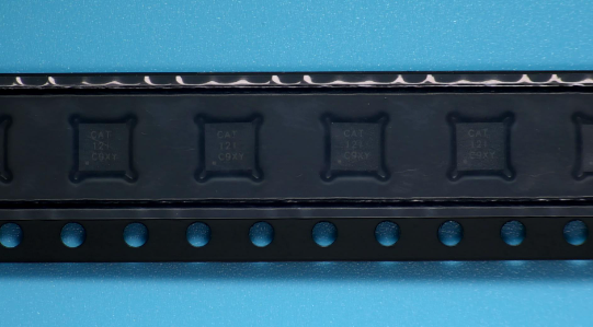
| CATALOG |
TPS62410DRCR COUNTRY OF ORIGIN
|
TPS62410DRCR PARAMETRIC INFO
|
TPS62410DRCR PACKAGE INFO
|
TPS62410DRCR MANUFACTURING INFO
|
TPS62410DRCR PACKAGING INFO
|
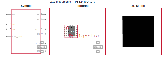
TPS62410DRCR ECAD MODELS
|
TPS62410DRCR APPLICATIONS
|
|
COUNTRY OF ORIGIN
|
China
|
Philippines
|
Thailand
|
Taiwan (Province of China)
|
Malaysia
|
|
PARAMETRIC INFO
|
| Type |
Synchronous Step Down |
| Number of Outputs |
2 |
| Minimum Input Voltage (V) |
2.5 |
| Maximum Input Voltage (V) |
6 |
| Output Voltage (V) |
0.6 to 6 |
| Maximum Output Current (A) |
0.8|0.8 |
| Minimum Operating Temperature (°C) |
-40 |
| Maximum Operating Temperature (°C) |
85 |
| Maximum Switching Frequency (kHz) |
2250(Typ) |
| Efficiency (%) |
95 |
| Switching Regulator |
Yes |
| Operating Supply Voltage Range (V) |
2.5 to 6 |
| Output Type |
Adjustable |
| Tradename |
EasyScale™ |
| Load Regulation |
0.5%/A |
| Typical Quiescent Current (uA) |
32 |
| Minimum Storage Temperature (°C) |
-65 |
| Maximum Storage Temperature (°C) |
150 |
| Typical Switch Current (A) |
1.2 |
|
| |
| PACKAGE INFO |
| Supplier Package |
VSON EP |
| Basic Package Type |
Non-Lead-Frame SMT |
| Pin Count |
10 |
| Lead Shape |
No Lead |
| PCB |
10 |
| Tab |
N/R |
| Pin Pitch (mm) |
0.5 |
| Package Length (mm) |
3.1(Max) |
| Package Width (mm) |
3.1(Max) |
| Package Height (mm) |
0.95(Max) |
| Package Diameter (mm) |
N/R |
| Package Overall Length (mm) |
3.1(Max) |
| Package Overall Width (mm) |
3.1(Max) |
| Package Overall Height (mm) |
1(Max) |
| Seated Plane Height (mm) |
1(Max) |
| Mounting |
Surface Mount |
| Terminal Width (mm) |
0.3(Max) |
| Package Weight (g) |
N/A |
| Package Material |
Plastic |
| Package Description |
Very Thin Small Outline No Lead, Exposed Pad |
| Package Family Name |
SON |
| Jedec |
N/A |
| Package Outline |
Link to Datasheet |
|
| |
| MANUFACTURING INFO |
| MSL |
2 |
| Maximum Reflow Temperature (°C) |
260 |
| Reflow Solder Time (Sec) |
30 |
| Number of Reflow Cycle |
3 |
| Standard |
J-STD-020D |
| Reflow Temp. Source |
Link to Datasheet |
| Maximum Wave Temperature (°C) |
N/R |
| Wave Solder Time (Sec) |
N/R |
| Lead Finish(Plating) |
Au |
| Under Plating Material |
Pd over Ni |
| Terminal Base Material |
Cu Alloy |
| Number of Wave Cycles |
N/R |
|
| |
| PACKAGING INFO |
| Packaging Suffix |
R |
| Packaging |
Tape and Reel |
| Quantity Of Packaging |
3000 |
| Reel Diameter (in) |
13 |
| Reel Width (mm) |
12.4 |
| Tape Pitch (mm) |
8 |
| Tape Width (mm) |
12 |
| Component Orientation |
Q2 |
| Packaging Document |
Link to Datasheet |
|
| |
| ECAD MODELS |
 |
|
| APPLICATIONS |
| • Cell Phones, Smartphones |
| • PDAs, Pocket PCs |
| • OMAP™ and Low-Power DSP Supply |
| • Portable Media Players |
| • Digital Radios |
| • Digital Cameras |
| |