|
|
• Input Voltage Range: 1.8 V to 5.5 V
|
• Fixed and Adjustable Output Voltage Options from 1.2 V to 5.5 V
|
• Up to 96% Efficiency
|
| • Up to 800-mA Output Current at 3.3 V in Boost Mode (VIN > 2.4 V) |
| • Automatic Transition Between Step-Down and Boost Mode |
| • Device Quiescent Current less than 50 μA
|
| • Power-Save Mode for Improved Efficiency at Low Output Power
|
| • Forced Fixed Frequency Operation and Synchronization Possible |
| • Load Disconnect During Shutdown |
| • Overtemperature Protection |
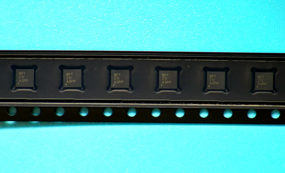
| • Available in a Small 3-mm × 3-mm 10-Pin VSON Package (QFN) |
|
| CATALOG |
TPS63000DRCR PARAMETRIC INFO
|
TPS63000DRCR PACKAGE INFO
|
TPS63000DRCR MANUFACTURING INFO
|
TPS63000DRCR PACKAGING INFO
|
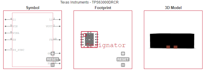
TPS63000DRCR ECAD MODELS
|
| TPS63000DRCR APPLICATIONS |
|
PARAMETRIC INFO
|
| Type |
Non-Inverting|Inverting|Step Up|Step Down |
| Number of Outputs |
1 |
| Minimum Input Voltage (V) |
1.8 |
| Maximum Input Voltage (V) |
5.5 |
| Output Voltage (V) |
1.2 to 5.5 |
| Maximum Output Current (A) |
1.2 |
| Minimum Operating Temperature (°C) |
-40 |
| Maximum Operating Temperature (°C) |
125 |
| Switching Frequency (kHz) |
1500 |
| Efficiency (%) |
96 |
| Switching Regulator |
Yes |
| Operating Supply Voltage (V) |
1.8 to 5.5 |
| Output Type |
Adjustable |
| Load Regulation |
0.5% |
| Line Regulation |
0.5% |
| Typical Quiescent Current (uA) |
40 |
| Typical Switch Current (A) |
1.8 |
|
|
PACKAGE INFO
|
| Supplier Package |
VSON EP |
| Basic Package Type |
Non-Lead-Frame SMT |
| Pin Count |
10 |
| Lead Shape |
No Lead |
| PCB |
10 |
| Tab |
N/R |
| Pin Pitch (mm) |
0.5 |
| Package Length (mm) |
3.1(Max) |
| Package Width (mm) |
3.1(Max) |
| Package Height (mm) |
0.95(Max) |
| Package Diameter (mm) |
N/R |
| Package Overall Length (mm) |
3.1(Max) |
| Package Overall Width (mm) |
3.1(Max) |
| Package Overall Height (mm) |
1(Max) |
| Seated Plane Height (mm) |
1(Max) |
| Mounting |
Surface Mount |
| Package Weight (g) |
N/A |
| Package Material |
Plastic |
| Package Description |
Very Thin Small Outline No Lead, Exposed Pad |
| Package Family Name |
SON |
| Package Outline |
Link to Datasheet |
|
|
MANUFACTURING INFO
|
| MSL |
2 |
| Maximum Reflow Temperature (°C) |
260 |
| Reflow Solder Time (Sec) |
30 |
| Number of Reflow Cycle |
3 |
| Standard |
J-STD-020D |
| Reflow Temp. Source |
Link to Datasheet |
| Maximum Wave Temperature (°C) |
N/R |
| Wave Solder Time (Sec) |
N/R |
| Lead Finish(Plating) |
Au |
| Under Plating Material |
Pd over Ni |
| Terminal Base Material |
Cu Alloy |
| Number of Wave Cycles |
N/R |
|
|
PACKAGING INFO
|
| Packaging Suffix |
R |
| Packaging |
Tape and Reel |
| Quantity Of Packaging |
3000 |
| Packaging Document |
Link to Datasheet |
|
|
ECAD MODELS
|
|
|
APPLICATIONS
|
• All Two-Cell and Three-Cell Alkaline, NiCd or
NiMH or Single-Cell Li Battery Powered Products
|
• Portable Audio Players
|
• Smart Phones
|
| • Personal Medical Products |
| • White LEDs |
| |