|
|
■ Stable with No Output Capacitor or Any Value or
voltage Type of Capacitor
|
■ Input Voltage Range of 1.7 V to 5.5 V
|
■ Ultra-Low Dropout Voltage: 75 mV typ
|
■ Excellent Load Transient Response—with or without Optional Output Capacitor
|
■ New NMOS Topology Delivers Low Reverse
Leakage Current
|
■ Less Than 1 μA max IQ in Shutdown Mode
|
■ Low Cost Due to Wafer-Level Trimming
|
■ 0.5% Initial Accuracy
|
■ Thermal Shutdown and Specified Min/Max
Current Limit Protection
|
|
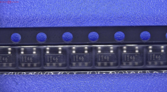
| CATALOG |
| TPS73633DBVR COUNTRY OF ORIGIN |
TPS73633DBVR PARAMETRIC INFO
|
TPS73633DBVR PACKAGE INFO
|
TPS73633DBVR MANUFACTURING INFO
|
| TPS73633DBVR PACKAGING INFO
|
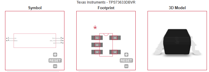
TPS73633DBVR ECAD MODELS
|
TPS73633DBVR APPLICATIONS
|
|
COUNTRY OF ORIGIN
|
| Malaysia |
China
|
Philippines
|
Thailand
|
|
PARAMETRIC INFO
|
| Type |
LDO |
| Number of Outputs |
1 |
| Maximum Output Current (A) |
0.4 |
| Minimum Operating Temperature (°C) |
-40 |
| Maximum Operating Temperature (°C) |
125 |
| Output Type |
Fixed |
| Output Voltage Range (V) |
1.8 to 10 |
| Regulation Condition Change In Load |
399mA |
| Regulation Condition Change In Line |
1.7V |
| Junction to Ambient |
221.9°C/W |
| Junction to Case |
74.9°C/W |
| Polarity |
Positive |
| Special Features |
Current Limit|Reverse Current Protection|Thermal Shutdown Protection |
| Process Technology |
BiCMOS |
| Load Regulation |
0.002%/mA(Typ) |
| Line Regulation |
0.01%/V(Typ) |
| Maximum Quiescent Current (mA) |
0.55 |
| Maximum Dropout Voltage @ Current (V) |
0.2@400mA |
| Minimum Input Voltage (V) |
1.7 |
| Maximum Input Voltage (V) |
5.5 |
| Output Voltage (V) |
3.3 |
| Typical Quiescent Current (mA) |
0.4 |
| Typical Dropout Voltage @ Current (V) |
0.075@400mA |
| Accuracy (%) |
±0.5 |
| Minimum Storage Temperature (°C) |
-65 |
| Maximum Storage Temperature (°C) |
150 |
| Typical Ground Current @ Full Load (mA) |
0.8 |
| Typical PSRR (dB) |
58 |
| Typical Output Capacitance (uF) |
0(Min) |
| Typical Output Noise Voltage (uVrms) |
30 |
| Pass Element Type |
NMOS |
|
|
PACKAGE INFO
|
| Supplier Package |
SOT-23 |
| Basic Package Type |
Lead-Frame SMT |
| Pin Count |
5 |
| Lead Shape |
Gull-wing |
| PCB |
5 |
| Tab |
N/R |
| Pin Pitch (mm) |
0.95 |
| Package Length (mm) |
3.05(Max) |
| Package Width (mm) |
1.75(Max) |
| Package Height (mm) |
1.1 |
| Package Diameter (mm) |
N/R |
| Package Overall Length (mm) |
3.05(Max) |
| Package Overall Width (mm) |
3(Max) |
| Package Overall Height (mm) |
1.45(Max) |
| Seated Plane Height (mm) |
1.45(Max) |
| Mounting |
Surface Mount |
| Package Weight (g) |
N/A |
| Package Material |
Plastic |
| Package Description |
Small Outline Transistor |
| Package Family Name |
SOT |
| Jedec |
MO-178 |
|
|
MANUFACTURING INFO
|
| MSL |
1 |
| Maximum Reflow Temperature (°C) |
260 |
| Reflow Solder Time (Sec) |
30 |
| Number of Reflow Cycle |
3 |
| Standard |
J-STD-020D |
| Reflow Temp. Source |
Link to Datasheet |
| Maximum Wave Temperature (°C) |
260 |
| Wave Solder Time (Sec) |
4 |
| Wave Temp. Source |
Link to Datasheet |
| Lead Finish(Plating) |
Au |
| Under Plating Material |
Pd over Ni |
| Terminal Base Material |
Cu Alloy |
| Number of Wave Cycles |
N/A |
|
|
PACKAGING INFO
|
| Packaging Suffix |
R |
| Packaging |
Tape and Reel |
| Quantity Of Packaging |
3000 |
| Reel Diameter (in) |
7 |
| Reel Width (mm) |
9 |
| Tape Pitch (mm) |
4 |
| Tape Width (mm) |
8 |
| Component Orientation |
Q3 |
| Packaging Document |
Link to Datasheet |
|
|
ECAD MODELS
|
|
|
APPLICATIONS
|
• Portable/Battery-Powered Equipment
|
• Post-Regulation for Switching Supplies
|
• Noise-Sensitive Circuitry such as VCOs
|
| • Point of Load Regulation for DSPs, FPGAs,
ASICs, and Microprocessors |
|