|
|
• Stable with 1μF or larger ceramic output capacitor
|
• Input voltage range: 2.2V to 5.5V
|
• Ultra-low dropout voltage– Legacy silicon: 130mV typical at 1A– New silicon: 122mV typical at 1A
|
• Excellent load transient response—even with only 1μF output capacitor
|
|
| CATALOG |
TPS73733DCQR COUNTRY OF ORIGIN
|
TPS73733DCQR PARAMETRIC INFO
|
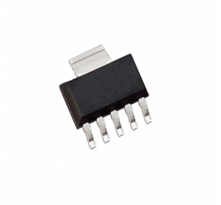
TPS73733DCQR PACKAGE INFO
|
TPS73733DCQR MANUFACTURING INFO
|
TPS73733DCQR PACKAGING INFO
|
TPS73733DCQR ECAD MODELS
|
TPS73733DCQR APPLICATIONS
|
|
COUNTRY OF ORIGIN
|
China
|
Thailand
|
Malaysia
|
|
PARAMETRIC INFO
|
| Type |
LDO |
| Number of Outputs |
1 |
| Maximum Output Current (A) |
1 |
| Minimum Operating Temperature (°C) |
-40 |
| Maximum Operating Temperature (°C) |
125 |
| Output Type |
Fixed |
| Output Voltage Range (V) |
1.8 to 10 |
| Junction to Ambient |
53.1°C/W |
| Junction to Case |
35.2°C/W |
| Polarity |
Positive |
| Special Features |
Current Limit|Fault Protection|Thermal Shutdown Protection |
| Process Technology |
NMOS |
| Load Regulation |
0.002%/mA(Typ) |
| Line Regulation |
0.01%/V(Typ) |
| Maximum Dropout Voltage @ Current (V) |
0.5@1A |
| Minimum Input Voltage (V) |
2.2 |
| Maximum Input Voltage (V) |
5.5 |
| Output Voltage (V) |
3.3 |
| Typical Quiescent Current (mA) |
0.4 |
| Typical Dropout Voltage @ Current (V) |
0.13@1A |
| Reference Voltage (V) |
1.204(Typ) |
| Accuracy (%) |
±1 |
| Minimum Storage Temperature (°C) |
-65 |
| Maximum Storage Temperature (°C) |
150 |
| Typical PSRR (dB) |
58 |
| Typical Output Capacitance (uF) |
1(Min) |
| Typical Output Noise Voltage (uVrms) |
48 |
| Pass Element Type |
NMOS |
| Output Capacitor Type |
Ceramic |
|
|
PACKAGE INFO
|
| Supplier Package |
SOT-223 |
| Basic Package Type |
Lead-Frame SMT |
| Pin Count |
6 |
| Lead Shape |
Gull-wing |
| PCB |
5 |
| Tab |
Tab |
| Pin Pitch (mm) |
1.27 |
| Package Length (mm) |
6.55(Max) |
| Package Width (mm) |
3.55(Max) |
| Package Height (mm) |
1.65(Max) |
| Package Diameter (mm) |
N/R |
| Seated Plane Height (mm) |
1.8(Max) |
| Mounting |
Surface Mount |
| Package Weight (g) |
N/A |
| Package Material |
Plastic |
| Package Description |
Small Outline Transistor |
| Package Family Name |
SOT |
| Jedec |
MS-012AA |
| Package Outline |
Link to Datasheet |
|
|
MANUFACTURING INFO
|
| MSL |
2 |
| Maximum Reflow Temperature (°C) |
260 |
| Reflow Solder Time (Sec) |
30 |
| Number of Reflow Cycle |
3 |
| Standard |
J-STD-020D |
| Reflow Temp. Source |
Link to Datasheet |
| Maximum Wave Temperature (°C) |
N/R |
| Wave Solder Time (Sec) |
N/R |
| Lead Finish(Plating) |
Matte Sn |
| Under Plating Material |
N/A |
| Terminal Base Material |
Cu Alloy |
|
|
PACKAGING INFO
|
| Packaging Suffix |
R |
| Packaging |
Tape and Reel |
| Quantity Of Packaging |
2500 |
| Reel Diameter (in) |
13 |
| Reel Width (mm) |
12.4 |
| Tape Pitch (mm) |
8 |
| Tape Width (mm) |
12 |
| Component Orientation |
Q3 |
| Packaging Document |
Link to Datasheet |
|
|
ECAD MODELS
|
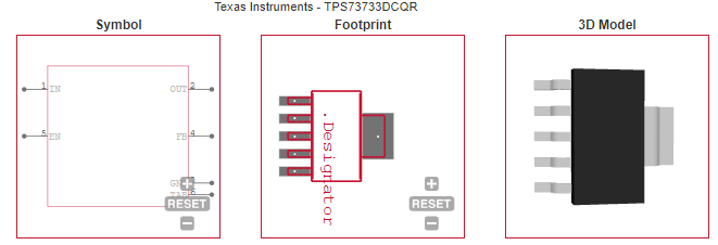 |
| |
| APPLICATIONS |
| • Point-of-load regulation for DSPs, FPGAs, ASICs, and microprocessors |
| • Post-regulation for switching supplies |
| |