
|
|
• Qualified for Automotive Applications
|
• Wide Input Voltage Range: 3 V to 50 V
|
• Low Quiescent Current: 40 μA (Typical)
|
• Low Dropout Voltage: 300 mV (Typical)
|
• Output Current: 50 mA
|
• No Input Protection Diodes Needed
|
• Adjustable Output From 1.275 V to 28 V
|
|
| CATALOG |
| TPS79801QDGNRQ1 COUNTRY OF ORIGIN |
TPS79801QDGNRQ1 PARAMETRIC INFO
|
TPS79801QDGNRQ1 PACKAGE INFO
|
TPS79801QDGNRQ1 MANUFACTURING INFO
|
TPS79801QDGNRQ1 PACKAGING INFO
|
TPS79801QDGNRQ1 ECAD MODELS
|
TPS79801QDGNRQ1 APPLICATIONS
|
|
COUNTRY OF ORIGIN
|
| Thailand |
China
|
|
PARAMETRIC INFO
|
| Type |
LDO |
| Number of Outputs |
1 |
| Maximum Output Current (A) |
0.05 |
| Minimum Operating Temperature (°C) |
-40 |
| Maximum Operating Temperature (°C) |
125 |
| Output Type |
Adjustable |
| Output Voltage Range (V) |
<1.8|1.8 to 10|10 to 20|20 to 50 |
| Junction to Ambient |
60°C/W |
| Junction to Case |
8.2°C/W |
| Polarity |
Positive |
| Special Features |
Current Limit|Reverse Battery Protection|Reverse Current Protection|Shutdown|Thermal Protection |
| Load Regulation |
20mV |
| Line Regulation |
13mV |
| Maximum Dropout Voltage @ Current (V) |
0.15@1mA|0.26@10mA|0.37@50mA |
| Maximum Power Dissipation (mW) |
1830 |
| Minimum Input Voltage (V) |
-65 |
| Maximum Input Voltage (V) |
50 |
| Output Voltage (V) |
1.275 to 28 |
| Typical Quiescent Current (mA) |
0.04 |
| Typical Dropout Voltage @ Current (V) |
0.085@1mA|0.17@10mA|0.3@50mA |
| Reference Voltage (V) |
1.275 |
| Accuracy (%) |
±3 |
| Minimum Storage Temperature (°C) |
-65 |
| Maximum Storage Temperature (°C) |
150 |
| Typical PSRR (dB) |
65 |
| Typical Output Capacitance (uF) |
1 |
| Typical Output Noise Voltage (uVrms) |
100 |
| Output Capacitor Type |
Ceramic|Tantalum|Aluminum |
|
|
PACKAGE INFO
|
| Supplier Package |
HVSSOP EP |
| Basic Package Type |
Lead-Frame SMT |
| Pin Count |
8 |
| Lead Shape |
Gull-wing |
| PCB |
8 |
| Tab |
N/R |
| Pin Pitch (mm) |
0.65 |
| Package Length (mm) |
3.1(Max) |
| Package Width (mm) |
3.1(Max) |
| Package Height (mm) |
0.95(Max) |
| Package Diameter (mm) |
N/R |
| Package Overall Length (mm) |
3.1(Max) |
| Package Overall Width (mm) |
5.05(Max) |
| Package Overall Height (mm) |
1.1(Max) |
| Seated Plane Height (mm) |
1.1(Max) |
| Mounting |
Surface Mount |
| Package Weight (g) |
N/A |
| Package Material |
Plastic |
| Package Description |
Heat Sinked Very Thin Shrink Small Outline Package, Exposed Pad |
| Package Family Name |
SOP |
| Jedec |
MO-187AA-T |
| Package Outline |
Link to Datasheet |
|
|
MANUFACTURING INFO
|
| MSL |
2 |
| Maximum Reflow Temperature (°C) |
260 |
| Reflow Solder Time (Sec) |
30 |
| Number of Reflow Cycle |
3 |
| Standard |
J-STD-020D |
| Reflow Temp. Source |
Link to Datasheet |
| Maximum Wave Temperature (°C) |
N/R |
| Wave Solder Time (Sec) |
N/R |
| Lead Finish(Plating) |
AuAg |
| Under Plating Material |
Pd over Ni |
| Terminal Base Material |
Cu Alloy |
| Number of Wave Cycles |
N/R |
|
|
PACKAGING INFO
|
| Packaging Suffix |
R |
| Packaging |
Tape and Reel |
| Quantity Of Packaging |
2500 |
| Reel Diameter (in) |
13 |
| Reel Width (mm) |
12.4 |
| Tape Pitch (mm) |
8 |
| Tape Width (mm) |
12 |
| Component Orientation |
Q1 |
| Packaging Document |
Link to Datasheet |
|
|
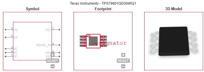
ECAD MODELS
|
|
|
APPLICATIONS
|
• Low-Current, High-Voltage Regulators
|
• Regulators for Battery-Powered Systems
|
• Telecom
|
• Automotives
|
|