 |
|
| • Input Voltage Range: –3 V to –35 V |
• Noise:
– 14 μVRMS (20 Hz to 20 kHz)
– 15.1 μVRMS (10 Hz to 100 kHz) |
• Power-Supply Ripple Rejection:
– 72 dB (120 Hz)
– ≥ 55 dB (10 Hz to 700 kHz) |
| • Adjustable Output: –1.18 V to –33 V |
| • Maximum Output Current: 200 mA |
| • Dropout Voltage: 216 mV at 100 mA |
| • Stable with Ceramic Capacitors ≥ 2.2 μF |
| • CMOS Logic-Level-Compatible Enable Pin |
| • Built-In, Fixed, Current Limit and Thermal Shutdown Protection |
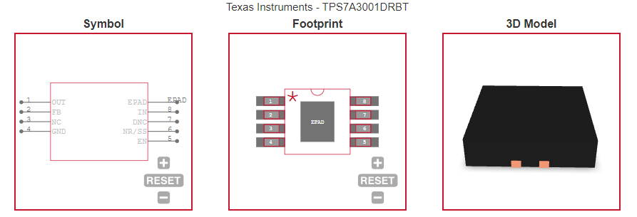
| • Packages: 8-Pin HVSSOP PowerPAD™ and 3-mm × 3-mm VSON |
| • Operating Temperature Range:–40°C to 125°C |
|
| CATALOG |
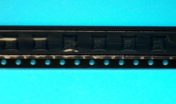
| TPS7A3001DRBT COUNTRY OF ORIGIN |
| TPS7A3001DRBT PARAMETRIC INFO |
| TPS7A3001DRBT PACKAGE INFO |
| TPS7A3001DRBT MANUFACTURING INFO |
| TPS7A3001DRBT PACKAGING INFO |
| TPS7A3001DRBT ECAD MODELS |
| TPS7A3001DRBT FUNCTIONAL BLOCK DIAGRAM |
| TPS7A3001DRBT APPLICATIONS |
|
| COUNTRY OF ORIGIN |
| Philippines |
|
| PARAMETRIC INFO |
| Type |
LDO |
| Number of Outputs |
1 |
| Maximum Output Current (A) |
0.2 |
| Minimum Operating Temperature (°C) |
-40 |
| Maximum Operating Temperature (°C) |
125 |
| Output Type |
Adjustable |
| Output Voltage Range (V) |
<1.8 |
| Regulation Condition Change In Load |
199mA |
| Junction to Ambient |
47.7°C/W |
| Junction to Case |
55.3°C/W |
| Polarity |
Negative |
| Special Features |
Current Limit|Thermal Shutdown Protection |
| Process Technology |
Bipolar |
| Load Regulation |
0.04%Vo(Typ) |
| Line Regulation |
0.14%Vo(Typ) |
| Maximum Dropout Voltage @ Current (V) |
0.6@200mA |
| Minimum Input Voltage (V) |
-35 |
| Maximum Input Voltage (V) |
-3 |
| Output Voltage (V) |
-1.18 to -33 |
| Typical Quiescent Current (mA) |
0.05 |
| Typical Dropout Voltage @ Current (V) |
0.216@100mA|0.325@200mA |
| Reference Voltage (V) |
-1.166 |
| Accuracy (%) |
±1.5 |
| Minimum Storage Temperature (°C) |
-65 |
| Maximum Storage Temperature (°C) |
150 |
| Typical Ground Current @ Full Load (mA) |
0.95 |
| Typical PSRR (dB) |
72 |
| Typical Output Capacitance (uF) |
2.2(Min) |
| Typical Output Noise Voltage (uVrms) |
17.5 |
| Output Capacitor Type |
Ceramic |
|
| |
| PACKAGE INFO |
| Supplier Package |
VSON EP |
| Basic Package Type |
Non-Lead-Frame SMT |
| Pin Count |
8 |
| Lead Shape |
No Lead |
| PCB |
8 |
| Tab |
N/R |
| Pin Pitch (mm) |
0.65 |
| Package Length (mm) |
3.15(Max) |
| Package Width (mm) |
3.15(Max) |
| Package Height (mm) |
0.95(Max) |
| Package Diameter (mm) |
N/R |
| Package Overall Length (mm) |
3.15(Max) |
| Package Overall Width (mm) |
3.15(Max) |
| Package Overall Height (mm) |
1(Max) |
| Seated Plane Height (mm) |
1(Max) |
| Mounting |
Surface Mount |
| Package Weight (g) |
N/A |
| Package Material |
Plastic |
| Package Description |
Very Thin Small Outline No Lead, Exposed Pad |
| Package Family Name |
SON |
| Jedec |
N/A |
|
| |
| MANUFACTURING INFO |
| MSL |
1 |
| Maximum Reflow Temperature (°C) |
260 |
| Reflow Solder Time (Sec) |
30 |
| Number of Reflow Cycle |
3 |
| Standard |
J-STD-020D |
| Reflow Temp. Source |
Link to Datasheet |
| Maximum Wave Temperature (°C) |
N/R |
| Wave Solder Time (Sec) |
N/R |
| Wave Temp. Source |
Link to Datasheet |
| Lead Finish(Plating) |
Au |
| Under Plating Material |
Pd over Ni |
| Terminal Base Material |
Cu Alloy |
| Number of Wave Cycles |
N/R |
|
| |
| PACKAGING INFO |
| Packaging Suffix |
T |
| Packaging |
Tape and Reel |
| Quantity Of Packaging |
250 |
| Reel Diameter (in) |
7.09 |
| Reel Width (mm) |
12.4 |
| Tape Pitch (mm) |
8 |
| Tape Width (mm) |
12 |
| Component Orientation |
Q2 |
| Packaging Document |
Link to Datasheet |
|
| |
| ECAD MODELS |
 |
|
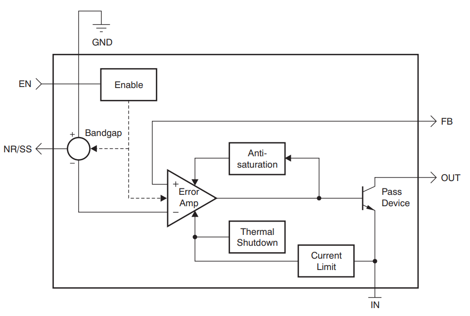
| FUNCTIONAL BLOCK DIAGRAM |
 |
|
| APPLICATIONS |
| • Supply Rails for Operational Amplifiers, DACs, ADCs, and Other High-Precision Analog Circuitry |
| • Audio |
| • Post DC-DC Converter Regulation and Ripple Filtering |
| • Test and Measurement |
| • RX, TX, and PA Circuitry |
| • Industrial Instrumentation |
| • Base Stations and Telecom Infrastructure |
| • –12-V and –24-V Industrial Buses |
| |
| |