 |
|
| • Wide Input Voltage Range: 7 V to 50 V |
• Accuracy:
– Nominal: 1%
– Over Line, Load, and Temperature: 2.5% |
| • Low Quiescent Current: 25 µA |
| • Quiescent Current at Shutdown: 4.1 µA |
| • Maximum Output Current: 50 mA |
| • CMOS Logic-Level-Compatible Enable Pin |
| • Adjustable Output Voltage: about 1.175 V to 48 V |
• Stable with Ceramic Capacitors:
– Input Capacitance: ≥ 1 µF
– Output Capacitance: ≥ 4.7 µF |
| • Dropout Voltage: 290 mV |
| • Built-In Current Limit and Thermal Shutdown
Protection |
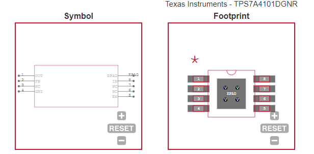
| • Package: High Thermal Performance HVSSOP-8
PowerPAD™ |
| • Operating Temperature Range: –40°C to 125°C |
|
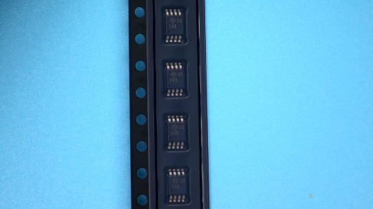
| CATALOG |
| TPS7A4101DGNR COUNTRY OF ORIGIN |
| TPS7A4101DGNR PARAMETRIC INFO |
| TPS7A4101DGNR PACKAGE INFO |
| TPS7A4101DGNR MANUFACTURING INFO |
| TPS7A4101DGNR PACKAGING INFO |
| TPS7A4101DGNR ECAD MODELS |
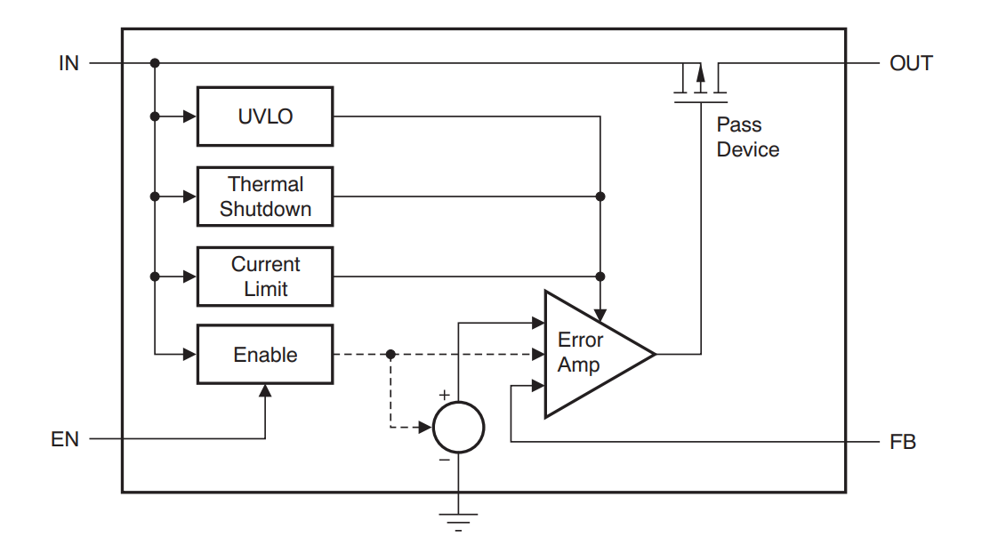
| TPS7A4101DGNR FUNCTIONAL BLOCK DIAGRAM |
| TPS7A4101DGNR APPLICATIONS |
|
| COUNTRY OF ORIGIN |
| Thailand |
|
| PARAMETRIC INFO |
| Type |
LDO |
| Number of Outputs |
1 |
| Maximum Output Current (A) |
0.05 |
| Minimum Operating Temperature (°C) |
-40 |
| Maximum Operating Temperature (°C) |
125 |
| Output Type |
Adjustable |
| Output Voltage Range (V) |
<1.8|1.8 to 10|10 to 20|20 to 50 |
| Junction to Ambient |
55.9°C/W |
| Junction to Case |
8.47°C/W |
| Polarity |
Positive |
| Special Features |
Current Limit|Thermal Shutdown Protection |
| Load Regulation |
0.31%Vo(Typ) |
| Line Regulation |
0.03%Vo(Typ) |
| Maximum Dropout Voltage @ Current (V) |
1.3@50mA |
| Maximum Power Dissipation (mW) |
1830 |
| Minimum Input Voltage (V) |
7 |
| Maximum Input Voltage (V) |
50 |
| Output Voltage (V) |
1.161 to 48 |
| Typical Quiescent Current (mA) |
0.025 |
| Typical Dropout Voltage @ Current (V) |
0.29@20mA|0.78@50mA |
| Reference Voltage (V) |
1.185 |
| Accuracy (%) |
±1 |
| Minimum Storage Temperature (°C) |
-65 |
| Maximum Storage Temperature (°C) |
150 |
| Typical PSRR (dB) |
38 |
| Typical Output Capacitance (uF) |
4.7(Min) |
|
| |
| PACKAGE INFO |
| Supplier Package |
HVSSOP EP |
| Basic Package Type |
Lead-Frame SMT |
| Pin Count |
8 |
| Lead Shape |
Gull-wing |
| PCB |
8 |
| Tab |
N/R |
| Pin Pitch (mm) |
0.65 |
| Package Length (mm) |
3.1(Max) |
| Package Width (mm) |
3.1(Max) |
| Package Height (mm) |
0.95(Max) |
| Package Diameter (mm) |
N/R |
| Package Overall Length (mm) |
3.1(Max) |
| Package Overall Width (mm) |
5.05(Max) |
| Package Overall Height (mm) |
1.1(Max) |
| Seated Plane Height (mm) |
1.1(Max) |
| Mounting |
Surface Mount |
| Package Weight (g) |
N/A |
| Package Material |
Plastic |
| Package Family Name |
SO |
| Package Outline |
Link to Datasheet |
|
| |
| MANUFACTURING INFO |
| MSL |
1 |
| Maximum Reflow Temperature (°C) |
260 |
| Reflow Solder Time (Sec) |
30 |
| Number of Reflow Cycle |
3 |
| Standard |
J-STD-020D |
| Reflow Temp. Source |
Link to Datasheet |
| Maximum Wave Temperature (°C) |
N/R |
| Wave Solder Time (Sec) |
N/R |
| Lead Finish(Plating) |
Au |
| Under Plating Material |
Pd over Ni |
| Terminal Base Material |
Cu Alloy |
|
| |
| PACKAGING INFO |
| Packaging Suffix |
R |
| Packaging |
Tape and Reel |
| Quantity Of Packaging |
2500 |
|
| |
| ECAD MODELS |
 |
|
| FUNCTIONAL BLOCK DIAGRAM |
 |
|
| APPLICATIONS |
| • Microprocessors, Microcontrollers Powered by
Industrial Busses with High Voltage Transients |
| • Industrial Automation
|
| • Telecom Infrastrucure |
| • Automotive |
| • LED Lighting
|
| • Bias Power Supplies |
| |
|