|
|
• Qualified for Automotive Applications
|
• AEC-Q100 Qualified for Automotive Applications:– Temperature Grade 1: –40°C ≤ TA ≤ +125°C– HBM ESD Classification Level 2– CDM ESD Classification Level C4A
|
• Extended Junction Temperature (TJ) Range:–40°C to +150°C
|
• Input Voltage Range:– Without BIAS: 1.4 V to 6.5 V– With BIAS: 1.1 V to 6.5 V
|
• Adjustable Output Voltage Range: 0.8 V to 5.2 V
|
• Low Dropout: 115 mV (max) at 2 A With BIAS
|
• Output Voltage Noise: 4.4 µVRMS
|
• 1% (max) Accuracy Over Line, Load, and Temperature With BIAS
|
|
| CATALOG |
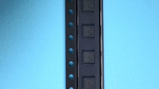
TPS7A5201QRGRRQ1 COUNTRY OF ORIGIN
|
TPS7A5201QRGRRQ1 PARAMETRIC INFO
|
TPS7A5201QRGRRQ1 PACKAGE INFO
|
TPS7A5201QRGRRQ1 MANUFACTURING INFO
|
TPS7A5201QRGRRQ1 PACKAGING INFO
|
TPS7A5201QRGRRQ1 ECAD MODELS
|
TPS7A5201QRGRRQ1 APPLICATIONS
|
|
COUNTRY OF ORIGIN
|
China
|
|
PARAMETRIC INFO
|
| Type |
LDO |
| Number of Outputs |
1 |
| Maximum Output Current (A) |
2 |
| Minimum Operating Temperature (°C) |
-40 |
| Maximum Operating Temperature (°C) |
150 |
| Output Type |
Adjustable |
| Output Voltage Range (V) |
<1.8|1.8 to 10 |
| Junction to Ambient |
43.4°C/W |
| Junction to Case |
36.8°C/W |
| Polarity |
Positive |
| Special Features |
Current Limit|Thermal Protection |
| Load Regulation |
0.08mV/A(Typ) |
| Line Regulation |
0.03mV/V(Typ) |
| Maximum Dropout Voltage @ Current (V) |
0.19@2A|0.22@2A|0.3@2A|0.12@2A |
| Minimum Input Voltage (V) |
1.1 |
| Maximum Input Voltage (V) |
6.5 |
| Output Voltage (V) |
0.8 to 5 |
| Typical Dropout Voltage @ Current (V) |
0.103@2A|0.135@2A|0.157@2A|0.073@2A |
| Accuracy (%) |
±1 |
| Supplier Temperature Grade |
Automotive |
| Minimum Storage Temperature (°C) |
-55 |
| Maximum Storage Temperature (°C) |
150 |
| Typical Bias Voltage (VDC) |
3 to 6.5 |
| Typical PSRR (dB) |
42 |
| Typical Output Noise Voltage (uVrms) |
7.7 |
| Output Capacitor Type |
Ceramic |
|
|
PACKAGE INFO
|
| Supplier Package |
VQFN EP |
| Basic Package Type |
Non-Lead-Frame SMT |
| Pin Count |
20 |
| Lead Shape |
No Lead |
| PCB |
20 |
| Tab |
N/R |
| Pin Pitch (mm) |
0.5 |
| Package Length (mm) |
3.65(Max) |
| Package Width (mm) |
3.65(Max) |
| Package Height (mm) |
0.95(Max) |
| Package Diameter (mm) |
N/R |
| Package Overall Length (mm) |
3.65(Max) |
| Package Overall Width (mm) |
3.65(Max) |
| Package Overall Height (mm) |
1(Max) |
| Seated Plane Height (mm) |
1(Max) |
| Mounting |
Surface Mount |
| Package Weight (g) |
N/A |
| Package Material |
Plastic |
| Package Description |
Very Thin Quad Flat No Lead Package, Exposed Pad |
| Package Family Name |
QFN |
| Jedec |
N/A |
| Package Outline |
Link to Datasheet |
|
|
MANUFACTURING INFO
|
| MSL |
2 |
| Maximum Reflow Temperature (°C) |
260 |
| Reflow Solder Time (Sec) |
30 |
| Number of Reflow Cycle |
3 |
| Standard |
J-STD-020D |
| Reflow Temp. Source |
Link to Datasheet |
| Maximum Wave Temperature (°C) |
N/R |
| Wave Solder Time (Sec) |
N/R |
| Lead Finish(Plating) |
Au |
| Under Plating Material |
Pd over Ni |
| Terminal Base Material |
Cu |
| Number of Wave Cycles |
N/R |
|
|
PACKAGING INFO
|
| Packaging Suffix |
R |
| Packaging |
Tape and Reel |
| Quantity Of Packaging |
3000 |
| Reel Diameter (in) |
13 |
| Reel Width (mm) |
12.4 |
| Tape Pitch (mm) |
8 |
| Tape Width (mm) |
12 |
| Component Orientation |
Q2 |
| Packaging Document |
Link to Datasheet |
|
|
ECAD MODELS
|
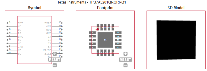
|
|
APPLICATIONS
|
• Telematic Control Units
|
• Infotainment and Clusters
|
• High-Speed Interfaces (PLL and VCO)
|
|