|
| |
• Low input offset voltage: 1.5 mV max. (A grade)
|
• Rail-to-rail input and output
|
• Wide bandwidth 20 MHz
|
| • Stable for gain ≥ 4 or ≤ -3 |
| • Low power consumption: 820 µA typ. |
| • High output current: 35 mA |
| • Operating from 2.5 V to 5.5 V |
| • Low input bias current, 1 pA typ. |
| • ESD internal protection ≥ 5 kV |
| |
| CATALOG |
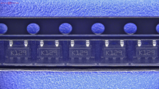
| TSV991AILT COUNTRY OF ORIGIN |
TSV991AILT PARAMETRIC INFO
|
TSV991AILT PACKAGE INFO
|
TSV991AILT MANUFACTURING INFO
|
TSV991AILT PACKAGING INFO
|
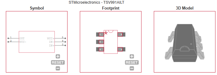
TSV991AILT EACD MODELS
|
| TSV991AILT APPLICATIONS |
|
| COUNTRY OF ORIGIN |
| China |
| Malaysia |
|
PARAMETRIC INFO
|
| Manufacturer Type |
Low Voltage Amplifier |
| Type |
Low Voltage Amplifier |
| Rail to Rail |
Rail to Rail Input/Output |
| Minimum Single Supply Voltage (V) |
2.5 |
| Number of Channels per Chip |
1 |
| Typical Single Supply Voltage (V) |
3|5 |
| Maximum Single Supply Voltage (V) |
5.5 |
| Output Type |
CMOS |
| Maximum Quiescent Current (mA) |
1.1@5V |
| Typical Gain Bandwidth Product (MHz) |
20 |
| Maximum Input Offset Voltage (mV) |
1.5@5V |
| Maximum Input Offset Current (uA) |
0.00001@5V |
| Maximum Operating Supply Voltage (V) |
5.5 |
| Maximum Input Bias Current (uA) |
0.00001@5V |
| Minimum CMRR (dB) |
62 |
| Maximum Supply Voltage Range (V) |
5.5 to 6 |
| Minimum CMRR Range (dB) |
60 to 65 |
| Typical Voltage Gain (dB) |
91 |
| Typical Slew Rate (V/us) |
10@5V |
| Typical Output Current (mA) |
35@5V |
| Typical Input Noise Voltage Density (nV/rtHz) |
21@5V |
| Shut Down Support |
No |
| Minimum Operating Temperature (°C) |
-40 |
| Maximum Operating Temperature (°C) |
125 |
| Minimum Storage Temperature (°C) |
-65 |
| Maximum Storage Temperature (°C) |
150 |
| Power Supply Type |
Single |
|
|
PACKAGE INFO
|
| Supplier Package |
SOT-23 |
| Basic Package Type |
Lead-Frame SMT |
| Pin Count |
5 |
| Lead Shape |
Gull-wing |
| PCB |
5 |
| Tab |
N/R |
| Pin Pitch (mm) |
0.95 |
| Package Length (mm) |
3(Max) |
| Package Width (mm) |
1.75(Max) |
| Package Height (mm) |
1.3(Max) |
| Package Diameter (mm) |
N/R |
| Seated Plane Height (mm) |
1.45(Max) |
| Mounting |
Surface Mount |
| Package Material |
Plastic |
| Package Description |
Small Outline Transistor |
| Package Family Name |
SOT |
| Jedec |
MO-178AA |
| Package Outline |
Link to Datasheet |
|
|
MANUFACTURING INFO
|
| MSL |
1 |
| Maximum Reflow Temperature (°C) |
260 |
| Reflow Solder Time (Sec) |
30 |
| Number of Reflow Cycle |
3 |
| Standard |
IPC-1752 |
| Reflow Temp. Source |
Link to Datasheet |
| Maximum Wave Temperature (°C) |
N/R |
| Wave Solder Time (Sec) |
N/R |
| Wave Temp. Source |
Link to Datasheet |
| Lead Finish(Plating) |
Au |
| Under Plating Material |
Pd over Ni |
| Terminal Base Material |
Cu Alloy |
| Shelf Life Period |
2 Years |
| Number of Wave Cycles |
N/R |
|
|
PACKAGING INFO
|
| Packaging |
Tape and Reel |
| Quantity Of Packaging |
1000 |
|
|
ECAD MODELS
|
|
|
| APPLICATIONS |
| • Battery-powered applications |
| • Portable devices |
| • Signal conditioning and active filtering |
| • Medical instrumentation |
| • Automotive applications |
| |