 |
|
| • No direction-control signal needed |
• Maximum data rates:
– 24 Mbps (push pull)
– 2 Mbps (open drain) |
| • Available in the Texas Instruments NanoStar™
integrated circuit package |
| • 1.65 V to 3.6 V on A port and 2.3 V to 5.5 V on B
port (VCCA ≤ VCCB) |
| • VCC isolation feature: if either VCC input is at GND,
both ports are in the High-Impedance state |
| • No power-supply sequencing required: either VCCA
or VCCB can be ramped first |
| • Ioff supports partial-power-down mode operation |
| • Latch-up performance exceeds 100 mA per JESD
78, Class II |
• ESD protection exceeds JESD 22:
– A port:
• 2500-V Human-Body Model (A114-B)
• 250-V Machine Model (A115-A)
• 1500-V Charged-Device Model (C101)
– B port:
• 8-kV Human-Body Model (A114-B)
• 250-V Machine Model (A115-A)
• 1500-V Charged-Device Model (C101)
|
|
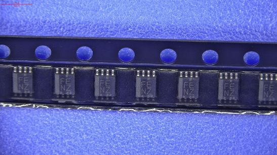
| CATALOG |
| TXS0102DCUR COUNTRY OF ORIGIN |
| TXS0102DCUR PARAMETRIC INFO |
| TXS0102DCUR PACKAGE INFO |
| TXS0102DCUR MANUFACTURING INFO |
| TXS0102DCUR PACKAGING INFO |
| TXS0102DCUR ECAD MODELS |
| TXS0102DCUR FUNCTIONAL BLOCK DIAGRAM |
| TXS0102DCUR APPLICATIONS |
|
| COUNTRY OF ORIGIN |
| China |
| Japan |
| Taiwan (Province of China) |
| Thailand |
|
| PARAMETRIC INFO |
| Number of Channels |
2 |
| Channel Type |
Bidirectional |
| Logic Family |
TXS |
| Logic Function |
Voltage Level Translator |
| Output Type |
3-State|Open Drain|Push-Pull |
| Minimum High Level Input Voltage (V) |
1.45 |
| Minimum Latch-Up Current (mA) |
100 |
| Minimum Operating Temperature (°C) |
-40 |
| Maximum Operating Temperature (°C) |
85 |
| Minimum Storage Temperature (°C) |
-65 |
| Maximum Storage Temperature (°C) |
150 |
| Minimum Operating Supply Voltage (V) |
1.65/2.3 |
| Maximum Operating Supply Voltage (V) |
3.6/5.5 |
| Typical Operating Supply Voltage (V) |
1.8/2.5|1.8/3.3|1.8/5|2.5|2.5/3.3|2.5/5|3.3|3.3/5 |
| Maximum High Level Output Current (mA) |
-0.02 |
| Maximum Low Level Output Current (mA) |
1 |
| Maximum Quiescent Current (mA) |
0.0144 |
| Maximum Propagation Delay Time @ Maximum CL (ns) |
260@1.65V to 1.95V@2.3V to 2.7V |
| Absolute Propagation Delay Time (ns) |
260 |
|
| |
| PACKAGE INFO |
| Supplier Package |
VSSOP |
| Basic Package Type |
Lead-Frame SMT |
| Pin Count |
8 |
| Lead Shape |
Gull-wing |
| PCB |
8 |
| Tab |
N/R |
| Pin Pitch (mm) |
0.5 |
| Package Length (mm) |
2.1(Max) |
| Package Width (mm) |
2.4(Max) |
| Package Height (mm) |
0.8(Max) |
| Package Diameter (mm) |
N/R |
| Package Overall Length (mm) |
2.1(Max) |
| Package Overall Width (mm) |
3.2(Max) |
| Package Overall Height (mm) |
0.9(Max) |
| Seated Plane Height (mm) |
0.9(Max) |
| Mounting |
Surface Mount |
| Package Weight (g) |
N/A |
| Package Material |
Plastic |
| Package Description |
Very Thin Shrink Small Outline Package |
| Package Family Name |
SOP |
| Jedec |
MO-187CA |
| Package Outline |
Link to Datasheet |
|
| |
| MANUFACTURING INFO |
| MSL |
1 |
| Maximum Reflow Temperature (°C) |
260 |
| Reflow Solder Time (Sec) |
30 |
| Number of Reflow Cycle |
3 |
| Standard |
J-STD-020D |
| Reflow Temp. Source |
Link to Datasheet |
| Maximum Wave Temperature (°C) |
N/R |
| Wave Solder Time (Sec) |
N/R |
| Lead Finish(Plating) |
Matte Sn|Au |
| Under Plating Material |
N/A|Pd over Ni |
| Terminal Base Material |
Cu |
| Number of Wave Cycles |
N/R |
|
| |
| PACKAGING INFO |
| Packaging Suffix |
R |
| Packaging |
Tape and Reel |
| Quantity Of Packaging |
3000 |
| Reel Diameter (in) |
7.09 |
| Reel Width (mm) |
8.4|9 |
| Tape Pitch (mm) |
4 |
| Tape Width (mm) |
8 |
| Component Orientation |
Q3 |
| Packaging Document |
Link to Datasheet |
|
| |
| ECAD MODELS |
 |
|
| FUNCTIONAL BLOCK DIAGRAM |
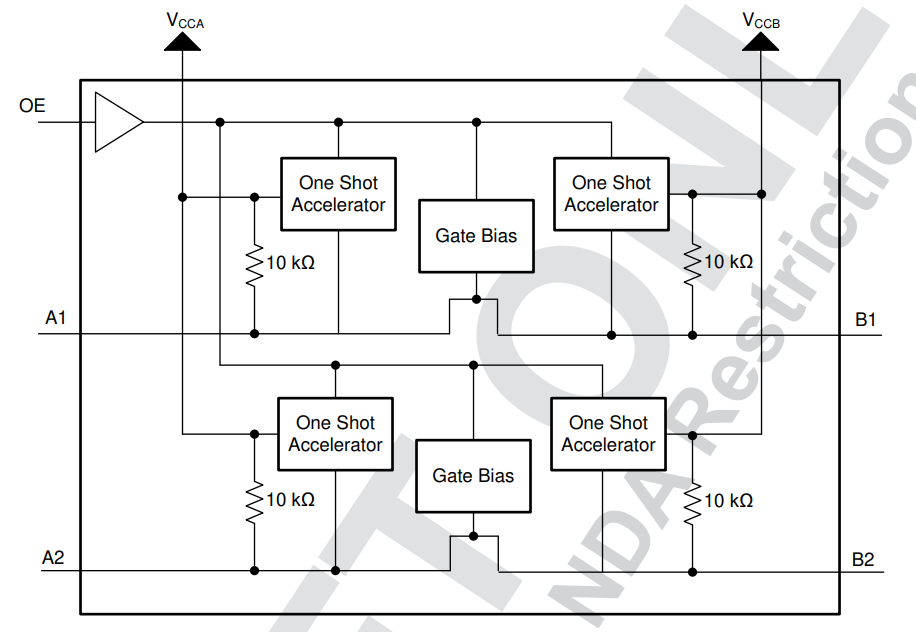 |
|
| APPLICATIONS |
| • I
2C / SMBus |
| • UART |
| • GPIO |
|