|
|
• 6-to-12 Demultiplexer/Multiplexer Allows SDIO Port Expansion
|
• Built-in Level Translator Eliminates Voltage Mismatch Between Baseband and SD Card or SDIO Peripheral
|
• VCCA, VCCB0, and VCCB1 Each Operate Over Full 1.1-V to 3.6-V Range
|
• Latch-Up Performance Exceeds 100 mA Per JESD 78, Class II
|
• ±8-kV Contact Discharge IEC 61000-4-2 ESD Performance (B Port)
|
|
| CATALOG |
TXS02612RTWR COUNTRY OF ORIGIN
|
TXS02612RTWR PARAMETRIC INFO
|
TXS02612RTWR PACKAGE INFO
|
TXS02612RTWR MANUFACTURING INFO
|
TXS02612RTWR PACKAGING INFO
|
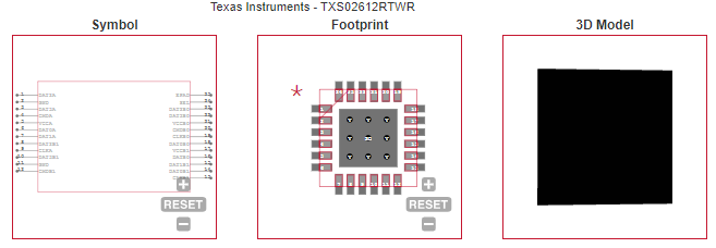
TXS02612RTWR ECAD MODELS
|
|
COUNTRY OF ORIGIN
|
China
|
Philippines
|
Thailand
|
Malaysia
|
|
PARAMETRIC INFO
|
| Number of Channels |
6 |
| Channel Type |
Bidirectional |
| Logic Family |
TXS |
| Logic Function |
Voltage Level Translator |
| Output Type |
Open Drain|Push-Pull |
| Minimum High Level Input Voltage (V) |
0.715 |
| Minimum Latch-Up Current (mA) |
100 |
| Minimum Operating Temperature (°C) |
-40 |
| Maximum Operating Temperature (°C) |
85 |
| Minimum Storage Temperature (°C) |
-65 |
| Maximum Storage Temperature (°C) |
150 |
| Minimum Operating Supply Voltage (V) |
1.1 |
| Maximum Operating Supply Voltage (V) |
3.6 |
| Typical Operating Supply Voltage (V) |
1.8|2.5|3.3 |
| Maximum High Level Output Current (mA) |
-8 |
| Maximum Low Level Output Current (mA) |
8 |
| Maximum Quiescent Current (mA) |
0.024 |
| Maximum Propagation Delay Time @ Maximum CL (ns) |
238(Typ)@1.2V |
| Absolute Propagation Delay Time (ns) |
780 |
|
|
PACKAGE INFO
|
| Supplier Package |
WQFN EP |
| Basic Package Type |
Non-Lead-Frame SMT |
| Pin Count |
24 |
| Lead Shape |
No Lead |
| PCB |
24 |
| Tab |
N/R |
| Pin Pitch (mm) |
0.5 |
| Package Length (mm) |
4.15(Max) |
| Package Width (mm) |
4.15(Max) |
| Package Height (mm) |
0.75(Max) |
| Package Diameter (mm) |
N/R |
| Package Overall Length (mm) |
4.15(Max) |
| Package Overall Width (mm) |
4.15(Max) |
| Package Overall Height (mm) |
0.8(Max) |
| Seated Plane Height (mm) |
0.8(Max) |
| Mounting |
Surface Mount |
| Terminal Width (mm) |
0.3(Max) |
| Package Weight (g) |
N/A |
| Package Material |
Plastic |
| Package Description |
Very Very Thin Quad Flat No Lead Package, Exposed Pad |
| Package Family Name |
QFN |
| Jedec |
MO-220 |
| Package Outline |
Link to Datasheet |
|
|
MANUFACTURING INFO
|
| MSL |
2 |
| Maximum Reflow Temperature (°C) |
260 |
| Reflow Solder Time (Sec) |
30 |
| Number of Reflow Cycle |
3 |
| Standard |
J-STD-020D |
| Reflow Temp. Source |
Link to Datasheet |
| Maximum Wave Temperature (°C) |
N/R |
| Wave Solder Time (Sec) |
N/R |
| Wave Temp. Source |
Link to Datasheet |
| Lead Finish(Plating) |
Au |
| Under Plating Material |
Pd over Ni |
| Terminal Base Material |
Cu Alloy |
| Number of Wave Cycles |
N/R |
|
|
PACKAGING INFO
|
| Packaging Suffix |
R |
| Packaging |
Tape and Reel |
| Quantity Of Packaging |
3000 |
| Reel Diameter (in) |
13 |
| Reel Width (mm) |
12.4 |
| Tape Pitch (mm) |
8 |
| Tape Width (mm) |
12 |
| Component Orientation |
Q2 |
| Packaging Document |
Link to Datasheet |
|
|
ECAD MODELS
|
 |
| |