 |
|
| • Qualified for Automotive Applications |
• AECA-Q100 Qualified with the following results:
– Device temperature grade –40°C to +140°C
– Device HBM classification level 2
– Device CDM classification level C6 |
| • 5-V Turn-off Under Voltage Lockout (UVLO) |
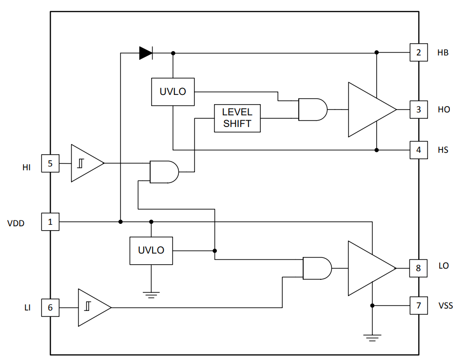
| • Drives Two N-Channel MOSFETs in High-Sideand Low-Side Configuration With IndependentInputs |
| • Maximum Boot Voltage 120-V DC |
| • 4-A Sink, 4-A Source Output Currents |
| • 0.9-Ω Pullup and Pulldown Resistance |
| • Input Pins Can Tolerate –10 V to +20 V and are
Independent of Supply Voltage Range
|
| • TTL Compatible Inputs |
| • 5-V to 17-V VDD Operating Range, (20-V ABS
Maximum) |
| • 7.2-ns Rise and 5.5-ns Fall Time With 1000-pF
Load |
| • Fast Propagation Delay Times (20-ns typical)
|
| • 4-ns Typical Delay Matching |
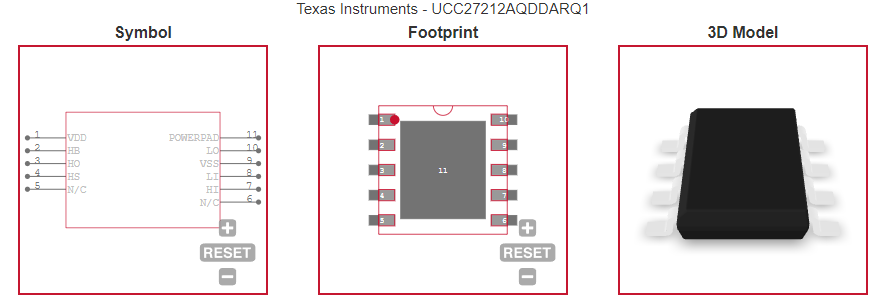
| • Available in the SOIC8(Powerpad) package |
|
| CATALOG |
| UCC27212AQDDARQ1 COUNTRY OF ORIGIN |
| UCC27212AQDDARQ1 PARAMETRIC INFO |
| UCC27212AQDDARQ1 PACKAGE INFO |
| UCC27212AQDDARQ1 MANUFACTURING INFO |
| UCC27212AQDDARQ1 PACKAGING INFO |
| UCC27212AQDDARQ1 ECAD MODELS |
| UCC27212AQDDARQ1 FUNCTIONAL BLOCK DIAGRAM |
| UCC27212AQDDARQ1 APPLICATIONS |
|
| COUNTRY OF ORIGIN |
| Mexico |
| China |
| Malaysia |
|
| PARAMETRIC INFO |
| Driver Type |
High and Low Side |
| Number of Drivers |
2 |
| Bridge Type |
Full Bridge|Half Bridge |
| Driver Configuration |
Inverting|Non-Inverting |
| Input Logic Compatibility |
TTL |
| Maximum Operating Supply Voltage (V) |
17 |
| Peak Output Current (A) |
4 |
| Minimum Operating Temperature (°C) |
-40 |
| Type |
IGBT|MOSFET |
| Maximum Operating Temperature (°C) |
140 |
| Maximum Turn-Off Delay Time (ns) |
9.5 |
| Maximum Turn-On Delay Time (ns) |
9.5 |
| High and Low Sides Dependency |
Independent |
| Number of Outputs |
2 |
| Minimum Operating Supply Voltage (V) |
7 |
| Typical Operating Supply Voltage (V) |
12 |
| Maximum Supply Current (mA) |
6.5 |
| Absolute Propagation Delay Time (ns) |
57 |
| Maximum Propagation Delay Time (ns) |
57 |
| Maximum Rise Time (ns) |
13(Typ) |
| Maximum Fall Time (ns) |
13(Typ) |
| Typical Input High Threshold Voltage (V) |
2.3 |
| Typical Input Low Threshold Voltage (V) |
1.6 |
| Latch-Up Proof |
No |
| Special Features |
Under Voltage Lockout |
| Minimum Storage Temperature (°C) |
-65 |
| Maximum Storage Temperature (°C) |
150 |
|
| |
| PACKAGE INFO |
| Supplier Package |
HSOIC EP |
| Basic Package Type |
Lead-Frame SMT |
| Pin Count |
8 |
| Lead Shape |
Gull-wing |
| PCB |
8 |
| Tab |
N/R |
| Pin Pitch (mm) |
1.27 |
| Package Length (mm) |
5(Max) |
| Package Width (mm) |
4(Max) |
| Package Height (mm) |
1.55(Max) |
| Package Diameter (mm) |
N/R |
| Package Overall Length (mm) |
5(Max) |
| Package Overall Width (mm) |
6.2(Max) |
| Package Overall Height (mm) |
1.7(Max) |
| Seated Plane Height (mm) |
1.7(Max) |
| Mounting |
Surface Mount |
| Package Weight (g) |
N/A |
| Package Material |
Plastic |
| Package Family Name |
SO |
| Jedec |
MS-012-BA |
|
| |
| MANUFACTURING INFO |
| MSL |
2 |
| Maximum Reflow Temperature (°C) |
260 |
| Reflow Solder Time (Sec) |
30 |
| Number of Reflow Cycle |
3 |
| Standard |
J-STD-020D |
| Reflow Temp. Source |
Link to Datasheet |
| Maximum Wave Temperature (°C) |
N/R |
| Wave Solder Time (Sec) |
N/R |
| Lead Finish(Plating) |
AuAg |
| Under Plating Material |
Pd over Ni |
| Terminal Base Material |
Cu Alloy |
|
| |
| PACKAGING INFO |
| Packaging Suffix |
R |
| Packaging |
Tape and Reel |
| Quantity Of Packaging |
2500 |
| Packaging Document |
Link to Datasheet |
|
| |
| ECAD MODELS |
 |
|
| FUNCTIONAL BLOCK DIAGRAM |
 |
|
| APPLICATIONS |
| • Power Supplies in Automotive Applications |
| • Half-Bridge and Full-Bridge Converters |
| • High-Voltage Synchronous-Buck Converters |
| • Two-Switch Forward Converters |
| • Push-Pull and Active-Clamp Forward Converters |
| • Class-D Audio Amplifiers |
| |
|