 |
||||||||||||||||||||||||||||||||||
| |
||||||||||||||||||||||||||||||||||
| ■ General – Very low standby current – 3.0 V CMOS compatible input – Optimized electromagnetic emission – Very low electromagnetic susceptibility – In compliance with the 2002/95/EC European directive – Fault reset standby pin (FR_Stby) – Optimized for LED application |
||||||||||||||||||||||||||||||||||
| ■ Diagnostic functions – Proportional load current sense – High current sense precision for wide range currents – Off-state open load detection – Output short to VCC detection – Overload and short to ground latch off – Thermal shutdown latch-off – Very low current sense leakage |
||||||||||||||||||||||||||||||||||
| ■ Protections – Undervoltage shutdown – Overvoltage clamp – Load current limitation – Self limiting of fast thermal transients – Protection against loss of ground and loss of VCC – Thermal shutdown – Electrostatic discharge protection |
||||||||||||||||||||||||||||||||||
| |
||||||||||||||||||||||||||||||||||
| CATALOG | ||||||||||||||||||||||||||||||||||
| VND5T035LAKTR-E COUNTRY OF ORIGIN | ||||||||||||||||||||||||||||||||||
| VND5T035LAKTR-E PARAMETRIC INFO | ||||||||||||||||||||||||||||||||||
| VND5T035LAKTR-E PACKAGE INFO | ||||||||||||||||||||||||||||||||||
| VND5T035LAKTR-E MANUFACTURING INFO | ||||||||||||||||||||||||||||||||||
| VND5T035LAKTR-E PACKAGING INFO | ||||||||||||||||||||||||||||||||||
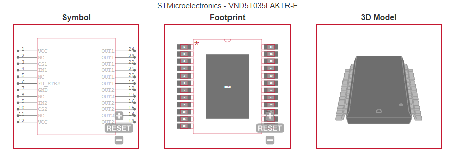
| VND5T035LAKTR-E ECAD MODELS | ||||||||||||||||||||||||||||||||||
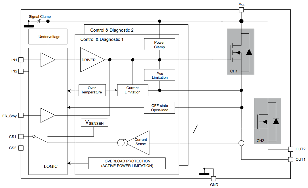
| VND5T035LAKTR-E FUNCTIONAL BLOCK DIAGRAM | ||||||||||||||||||||||||||||||||||
| VND5T035LAKTR-E APPLICATION | ||||||||||||||||||||||||||||||||||
| |
||||||||||||||||||||||||||||||||||
| COUNTRY OF ORIGIN | ||||||||||||||||||||||||||||||||||
| Malaysia | ||||||||||||||||||||||||||||||||||
| |
||||||||||||||||||||||||||||||||||
| PARAMETRIC INFO | ||||||||||||||||||||||||||||||||||
|
||||||||||||||||||||||||||||||||||
| PACKAGE INFO | ||||||||||||||||||||||||||||||||||
|
||||||||||||||||||||||||||||||||||
| MANUFACTURING INFO | ||||||||||||||||||||||||||||||||||
|
||||||||||||||||||||||||||||||||||
| PACKAGING INFO | ||||||||||||||||||||||||||||||||||
|
||||||||||||||||||||||||||||||||||
| ECAD MODELS | ||||||||||||||||||||||||||||||||||
 |
||||||||||||||||||||||||||||||||||
| |
||||||||||||||||||||||||||||||||||
| FUNCTIONAL BLOCK DIAGRAM | ||||||||||||||||||||||||||||||||||
 |
||||||||||||||||||||||||||||||||||
| APPLICATION | ||||||||||||||||||||||||||||||||||
| ■ All types of resistive, inductive and capacitive loads | ||||||||||||||||||||||||||||||||||