 |
| |
| • Linear current limitation |
| • Thermal shutdown
|
| • Short circuit protection |
| • Integrated clamp |
| • Low current drawn from input pin |
| • Diagnostic feedback through input pin |
| • ESD protection |
| • Direct access to the gate of the Power
MOSFET (analog driving) |
| • Compatible with standard Power MOSFET in
compliance with the 2002/95/EC European
Directive |
|
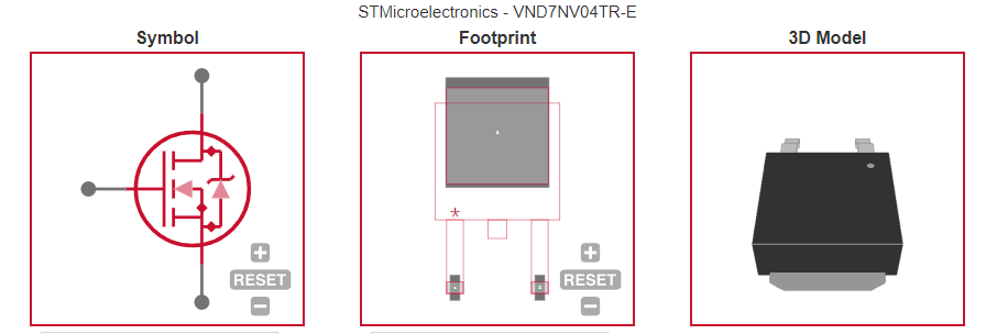
| CATALOG |
| VND7NV04TR-E Country of Origin |
| VND7NV04TR-E Parametric Info |
| VND7NV04TR-E Package Info |
| VND7NV04TR-E Manufacturing Info |
| VND7NV04TR-E Packaging Info |
| VND7NV04TR-E ECAD MODELS |
|
| COUNTRY OF ORIGIN |
| China |
| Malta |
| Morocco |
| United States of America |
|
| PARAMETRIC INFO |
| Number of Outputs |
1 |
| Number of Inputs |
1 |
| Maximum Output Current (A) |
12 |
| Switch On Resistance (mOhm) |
60(Max) |
| Maximum Power Dissipation (mW) |
60000 |
| Minimum Storage Temperature (°C) |
-55 |
| Maximum Storage Temperature (°C) |
150 |
|
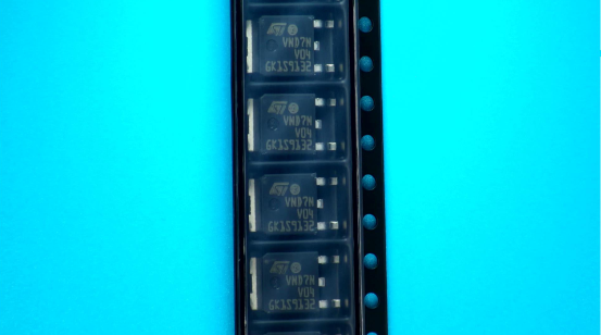
| PACKAGE INFO |
| Supplier Package |
DPAK |
| Pin Count |
3 |
| Lead Shape |
Gull-wing |
| PCB |
2 |
| Tab |
Tab |
| Pin Pitch (mm) |
2.3(Max) |
| Package Length (mm) |
6.6(Max) |
| Package Width (mm) |
6.2(Max) |
| Package Height (mm) |
2.4(Max) |
| Package Diameter (mm) |
N/R |
| Package Overall Length (mm) |
6.6(Max) |
| Package Overall Width (mm) |
10.1(Max) |
| Package Overall Height (mm) |
2.63(Max) |
| Seated Plane Height (mm) |
2.63(Max) |
| Mounting |
Surface Mount |
| Package Material |
Plastic |
| Package Description |
Deca Watt Package |
| Package Family Name |
TO-252 |
| Jedec |
TO-252AA |
| Package Outline |
Link to Datasheet |
|
| MANUFACTURING INFO |
| MSL |
3 |
| Maximum Reflow Temperature (°C) |
260 |
| Number of Reflow Cycle |
3 |
| Reflow Temp. Source |
Link to Datasheet |
| Maximum Wave Temperature (°C) |
N/R |
| Wave Solder Time (Sec) |
N/R |
| Wave Temp. Source |
Link to Datasheet |
| Lead Finish(Plating) |
Matte Sn annealed |
| Under Plating Material |
N/A |
| Terminal Base Material |
Cu Alloy |
| Shelf Life Period |
2 Years |
|
| PACKAGING INFO |
| Packaging Suffix |
TR |
| Packaging |
Tape and Reel |
| Quantity Of Packaging |
1000 |
| Packaging Document |
Link to Datasheet |
|
| ECAD MODELS |
 |
|