|
|
• Low-cost, high-performance logic solution for high-volume,
consumer-oriented applications
• Densities up to 74,880 logic cells
|
• SelectIO™ interface signaling
• Up to 633 I/O pins
• 622+ Mb/s data transfer rate per I/O
• 18 single-ended signal standards
• 8 differential I/O standards including LVDS, RSDS
• Termination by Digitally Controlled Impedance
• Signal swing ranging from 1.14V to 3.465V
• Double Data Rate (DDR) support
• DDR, DDR2 SDRAM support up to 333 Mb/s
|
• Logic resources
• Abundant logic cells with shift register capability
• Wide, fast multiplexers
• Fast look-ahead carry logic
• Dedicated 18 x 18 multipliers
• JTAG logic compatible with IEEE 1149.1/1532
|
• SelectRAM™ hierarchical memory
• Up to 1,872 Kbits of total block RAM
• Up to 520 Kbits of total distributed RAM
|
• Digital Clock Manager (up to four DCMs)
• Clock skew elimination
• Frequency synthesis
• High resolution phase shifting
|
| • Eight global clock lines and abundant routing |
| • Fully supported by Xilinx ISE® and WebPACK™ software
development systems |
| • MicroBlaze™ and PicoBlaze™ processor, PCI®,
PCI Express® PIPE Endpoint, and other IP cores |
| • Pb-free packaging options |
| • Automotive Spartan-3 XA Family variant |
|
| CATALOG |
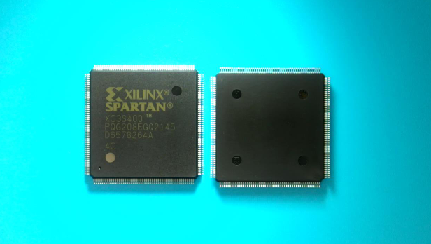
XC3S400-4PQG208C COUNTRY OF ORIGIN
|
XC3S400-4PQG208C PARAMETRIC INFO
|
XC3S400-4PQG208C PACKAGE INFO
|
XC3S400-4PQG208C MANUFACTURING INFO
|
XC3S400-4PQG208C PACKAGING INFO
|
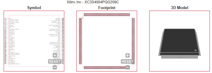
XC3S400-4PQG208C ECAD MODELS
|
|
COUNTRY OF ORIGIN
|
| United States of America |
| Taiwan (Province of China) |
| Philippines |
|
PARAMETRIC INFO
|
| Device Logic Gates |
400000 |
| Device System Gates |
400000 |
| Device Logic Units |
8064 |
| Device Logic Cells |
8064 |
| Maximum Number of User I/Os |
141 |
| Number of I/O Banks |
8 |
| Device Number of DLLs/PLLs |
4 |
| Number of Multipliers |
16 (18x18) |
| Number of Inter Dielectric Layers |
8 |
| Tradename |
Spartan |
| Maximum Differential I/O Pairs |
62 |
| Maximum I/O Performance |
622Mbps |
| RAM Bits (Kbit) |
288 |
| Total Number of Block RAM |
16 |
| Program Memory Type |
SRAM |
| Maximum Distributed RAM Bits |
57344 |
| Family Name |
Spartan®-3 |
| Process Technology |
90nm |
| Speed Grade |
4 |
| Differential I/O Standards Supported |
LVDS|LVPECL|RSDS|SSTL|HSTL |
| Single-Ended I/O Standards Supported |
LVTTL|LVCMOS|PCI|SSTL|HSTL|GTL|GTLP |
| JTAG Support (-) |
Yes |
| Maximum Supply Current (mA) |
110 |
| External Memory Interface |
DDR SDRAM|DDR2 SDRAM |
| Copy Protection |
No |
| Shift Registers |
Utilize LUT |
| Programmability |
No |
| In-System Programmability |
Yes |
| Number of Look-up Table Input |
4 |
| Reprogrammability Support |
Yes |
| Maximum Internal Frequency (MHz) |
630 |
| Number of Global Clocks |
8 |
| Maximum Operating Supply Voltage (V) |
1.26 |
| I/O Voltage (V) |
1.2|1.5|1.8|2.5|3.3 |
| Minimum Operating Temperature (°C) |
0 |
| Maximum Operating Temperature (°C) |
85 |
| Temperature Flag |
Jun |
| Supplier Temperature Grade |
Commercial |
| Digital Control Impedance |
Yes |
| Minimum Operating Supply Voltage (V) |
1.14 |
| Typical Operating Supply Voltage (V) |
1.2 |
| Tolerant Configuration Interface Voltage (V) |
3.3 |
| Maximum Storage Temperature (°C) |
150 |
| Minimum Storage Temperature (°C) |
-65 |
|
|
PACKAGE INFO
|
| Supplier Package |
PQFP EP |
| Basic Package Type |
Lead-Frame SMT |
| Pin Count |
208 |
| Lead Shape |
Gull-wing |
| PCB |
208 |
| Tab |
N/R |
| Pin Pitch (mm) |
0.5 |
| Package Length (mm) |
28 |
| Package Width (mm) |
28 |
| Package Height (mm) |
3.4 |
| Package Diameter (mm) |
N/R |
| Seated Plane Height (mm) |
3.7 |
| Mounting |
Surface Mount |
| Package Weight (g) |
N/A |
| Package Material |
Plastic |
| Package Description |
Plastic Quad Flat Package, Exposed Pad |
| Package Family Name |
QFP |
| Jedec |
MS-029FA-1 |
| Package Outline |
Link to Datasheet |
|
|
MANUFACTURING INFO
|
| MSL |
3 |
| Maximum Reflow Temperature (°C) |
245 |
| Reflow Solder Time (Sec) |
30 |
| Number of Reflow Cycle |
3 |
| Standard |
IPC-1752 |
| Reflow Temp. Source |
Link to Datasheet |
| Maximum Wave Temperature (°C) |
N/R |
| Wave Solder Time (Sec) |
N/R |
| Lead Finish(Plating) |
Matte Sn annealed |
| Under Plating Material |
N/A |
| Terminal Base Material |
Cu |
| Number of Wave Cycles |
N/R |
|
|
PACKAGING INFO
|
| Packaging |
Tray |
| Quantity Of Packaging |
24(Max) |
| Packaging Document |
Link to Datasheet |
|
|
ECAD MODELS
|
|
|
| |
| |