|
|
• Advanced high-performance FPGA logic based on real 6-input lookup table (LUT) technology configurable as distributed memory.
|
• 36 Kb dual-port block RAM with built-in FIFO logic for on-chip databuffering.
|
• High-performance SelectIO™ technology with support for DDR3interfaces up to 1,866 Mb/s.
|
• High-speed serial connectivity with built-in multi-gigabit transceiversfrom 600 Mb/s to max. rates of 6.6 Gb/s up to 28.05 Gb/s, offering aspecial low-power mode, optimized for chip-to-chip interfaces.
|
• A user configurable analog interface (XADC), incorporating dual12-bit 1MSPS analog-to-digital converters with on-chip thermal andsupply sensors.
|
• DSP slices with 25 x 18 multiplier, 48-bit accumulator, and pre-adderfor high-performance filtering, including optimized symmetriccoefficient filtering.
|
• Powerful clock management tiles (CMT), combining phase-lockedloop (PLL) and mixed-mode clock manager (MMCM) blocks for highprecision and low jitter.
|
• Quickly deploy embedded processing with MicroBlaze™ processor.
|
• Integrated block for PCI Express® (PCIe), for up to x8 Gen3Endpoint and Root Port designs.
|
• Wide variety of configuration options, including support forcommodity memories, 256-bit AES encryption with HMAC/SHA-256authentication, and built-in SEU detection and correction.
|
• Low-cost, wire-bond, bare-die flip-chip, and high signal integrity flipchip packaging offering easy migration between family members inthe same package. All packages available in Pb-free and selectedpackages in Pb option.
|
• Designed for high performance and lowest power with 28 nm,HKMG, HPL process, 1.0V core voltage process technology and0.9V core voltage option for even lower power.
|
|
| CATALOG |
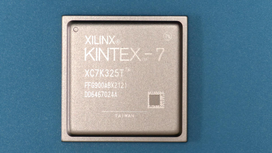
XC7K325T-2FFG900I COUNTRY OF ORIGIN
|
XC7K325T-2FFG900I PARAMETRIC INFO
|
XC7K325T-2FFG900I PACKAGE INFO
|
XC7K325T-2FFG900I MANUFACTURING INFO
|
XC7K325T-2FFG900I PACKAGING INFO
|
|
COUNTRY OF ORIGIN
|
Taiwan (Province of China)
|
|
PARAMETRIC INFO
|
| Device Logic Units |
326080 |
| Device Logic Cells |
326080 |
| Maximum Number of User I/Os |
350 |
| Number of I/O Banks |
10 |
| Device Number of DLLs/PLLs |
10 |
| Number of Multipliers |
840 (25x18) |
| Maximum LVDS Data Rate (Mbps) |
1250 |
| Number of Regional Clocks |
4 |
| Tradename |
Kintex |
| Number of Registers |
407600 |
| Maximum I/O Performance |
12.5Gbps |
| RAM Bits (Kbit) |
16020 |
| Total Number of Block RAM |
445 |
| Program Memory Type |
SRAM |
| Maximum Distributed RAM Bits |
4096000 |
| Family Name |
Kintex-7 |
| Process Technology |
28nm |
| Speed Grade |
2 |
| Transceiver Blocks |
16 |
| Transceiver Speed (Gbps) |
12.5 |
| Dedicated DSP |
840 |
| JTAG Support (-) |
Yes |
| PCI Blocks |
1 |
| Copy Protection |
Yes |
| Shift Registers |
Utilize LUT |
| Programmability |
Yes |
| In-System Programmability |
Yes |
| Number of Look-up Table Input |
6 |
| Reprogrammability Support |
Yes |
| Number of Global Clocks |
32 |
| Maximum Operating Supply Voltage (V) |
1.03 |
| I/O Voltage (V) |
1.2|1.35|1.5|1.8|2.5|3.3 |
| Minimum Operating Temperature (°C) |
-40 |
| Maximum Operating Temperature (°C) |
100 |
| Temperature Flag |
Jun |
| Supplier Temperature Grade |
Industrial |
| Digital Control Impedance |
No |
| Minimum Operating Supply Voltage (V) |
0.97 |
| Typical Operating Supply Voltage (V) |
1 |
| Maximum Storage Temperature (°C) |
150 |
| Minimum Storage Temperature (°C) |
-65 |
|
|
PACKAGE INFO
|
| Supplier Package |
FCBGA |
| Basic Package Type |
Ball Grid Array |
| Pin Count |
900 |
| Lead Shape |
Ball |
| PCB |
900 |
| Tab |
N/R |
| Pin Pitch (mm) |
1 |
| Package Length (mm) |
31 |
| Package Width (mm) |
31 |
| Package Height (mm) |
2.75(Max) |
| Package Diameter (mm) |
N/R |
| Seated Plane Height (mm) |
3.15 |
| Mounting |
Surface Mount |
| Package Material |
Plastic |
| Package Description |
Flip Chip Ball Grid Array |
| Package Family Name |
BGA |
| Package Outline |
Link to Datasheet |
|
|
MANUFACTURING INFO
|
| MSL |
4 |
| Maximum Reflow Temperature (°C) |
245 |
| Reflow Solder Time (Sec) |
30 |
| Number of Reflow Cycle |
3 |
| Reflow Temp. Source |
Link to Datasheet |
| Maximum Wave Temperature (°C) |
N/R |
| Wave Solder Time (Sec) |
N/R |
| Lead Finish(Plating) |
SnAgCu |
| Under Plating Material |
N/A |
| Terminal Base Material |
N/R |
|
|
PACKAGING INFO
|
| Packaging |
Tray |
| Quantity Of Packaging |
27 |
| Packaging Document |
Link to Datasheet |
|
|
|