 |
||||||||||||||||||||||||||||||||||||
| • In-System Programmable PROMs for Configuration of
Xilinx® FPGAs |
||||||||||||||||||||||||||||||||||||
| • Low-Power Advanced CMOS NOR Flash Process | ||||||||||||||||||||||||||||||||||||
| • Endurance of 20,000 Program/Erase Cycles | ||||||||||||||||||||||||||||||||||||
| • Operation over Full Industrial Temperature Range (–40°C to +85°C) | ||||||||||||||||||||||||||||||||||||
| • IEEE Standard 1149.1/1532 Boundary-Scan (JTAG) Support for Programming, Prototyping, and Testing | ||||||||||||||||||||||||||||||||||||
| • JTAG Command Initiation of Standard FPGA Configuration | ||||||||||||||||||||||||||||||||||||
| • Cascadable for Storing Longer or Multiple Bitstreams | ||||||||||||||||||||||||||||||||||||
| • Dedicated Boundary-Scan (JTAG) I/O Power Supply (VCCJ) | ||||||||||||||||||||||||||||||||||||
| • I/O Pins Compatible with Voltage Levels Ranging From 1.8V to 3.3V | ||||||||||||||||||||||||||||||||||||
| • Design Support Using the Xilinx ISE® Alliance and Foundation™ Software Packages | ||||||||||||||||||||||||||||||||||||
| • XCF01S/XCF02S/XCF04S • 3.3V Supply Voltage • Serial FPGA Configuration Interface • Available in Small-Footprint VO20 and VOG20 Packages |
||||||||||||||||||||||||||||||||||||
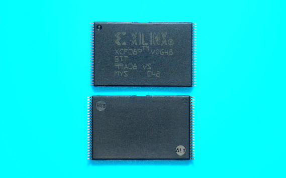
| • XCF08P/XCF16P/XCF32P • 1.8V Supply Voltage • Serial or Parallel FPGA Configuration Interface • Available in Small-Footprint VOG48, FS48, and FSG48 Packages • Design Revision Technology Enables Storing and Accessing Multiple Design Revisions for Configuration • Built-In Data Decompressor Compatible with Xilinx Advanced Compression Technology |
||||||||||||||||||||||||||||||||||||
| CATALOG |
||||||||||||||||||||||||||||||||||||
| XCF08PVOG48C COUNTRY OF ORIGIN | ||||||||||||||||||||||||||||||||||||
| XCF08PVOG48C PARAMETRIC INFO | ||||||||||||||||||||||||||||||||||||
| XCF08PVOG48C PACKAGE INFO | ||||||||||||||||||||||||||||||||||||
| XCF08PVOG48C MANUFACTURING INFO | ||||||||||||||||||||||||||||||||||||
| XCF08PVOG48C PACKAGING INFO | ||||||||||||||||||||||||||||||||||||
| COUNTRY OF ORIGIN | ||||||||||||||||||||||||||||||||||||
|
||||||||||||||||||||||||||||||||||||
| PARAMETRIC INFO |
||||||||||||||||||||||||||||||||||||
|
||||||||||||||||||||||||||||||||||||
| PACKAGE INFO | ||||||||||||||||||||||||||||||||||||
|
||||||||||||||||||||||||||||||||||||
| MANUFACTURING INFO | ||||||||||||||||||||||||||||||||||||
|
||||||||||||||||||||||||||||||||||||
| PACKAGING INFO | ||||||||||||||||||||||||||||||||||||
|
||||||||||||||||||||||||||||||||||||