|
|
• Low Input Capacitance
|
• Low On-Resistance
|
• Fast Switching Speed
|
• Lead-Free Finish; RoHS Compliant (Notes 1 & 2)
|
• Halogen and Antimony Free. “Green” Device (Note 3)
|
• For automotive applications requiring specific change control (i.e. parts qualified to AEC-Q100/101/104/200, PPAP capable,and manufactured in IATF 16949 certified facilities), please contact us or your local Diodes representative. https://www.diodes.com/quality/product-definitions/
|
|
| CATALOG |
ZXMP4A16GTA PARAMETRIC INFO
|
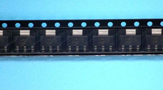
ZXMP4A16GTA PACKAGE INFO
|
ZXMP4A16GTA MANUFACTURING INFO
|
ZXMP4A16GTA PACKAGING INFO
|
ZXMP4A16GTA APPLICATIONS
|
|
PARAMETRIC INFO
|
| Channel Type |
P |
| Channel Mode |
Enhancement |
| Configuration |
Single Dual Drain |
| Maximum Drain Source Voltage (V) |
40 |
| Maximum Continuous Drain Current (A) |
4.6 |
| Maximum Gate Source Voltage (V) |
±20 |
| Maximum Drain Source Resistance (mOhm) |
60@10V |
| Typical Gate Charge @ Vgs (nC) |
13.6@5V|26.1@10V |
| Typical Gate Charge @ 10V (nC) |
26.1 |
| Maximum Power Dissipation (mW) |
3900 |
| Category |
Power MOSFET |
| Typical Input Capacitance @ Vds (pF) |
1007@20V |
| Typical Turn-On Delay Time (ns) |
2.33 |
| Typical Turn-Off Delay Time (ns) |
29.18 |
| Typical Fall Time (ns) |
12.54 |
| Typical Rise Time (ns) |
8.84 |
| Number of Elements per Chip |
1 |
| Minimum Storage Temperature (°C) |
-55 |
| Maximum Storage Temperature (°C) |
150 |
| Minimum Operating Temperature (°C) |
-55 |
| Maximum Operating Temperature (°C) |
150 |
|
|
PACKAGE INFO
|
| Supplier Package |
SOT-223 |
| Basic Package Type |
Lead-Frame SMT |
| Pin Count |
4 |
| Lead Shape |
Gull-wing |
| PCB |
3 |
| Tab |
Tab |
| Pin Pitch (mm) |
2.3 |
| Package Length (mm) |
6.5 |
| Package Width (mm) |
3.5 |
| Package Height (mm) |
1.6 |
| Package Diameter (mm) |
N/R |
| Package Overall Length (mm) |
6.5 |
| Package Overall Width (mm) |
7 |
| Package Overall Height (mm) |
1.65 |
| Seated Plane Height (mm) |
1.65 |
| Mounting |
Surface Mount |
| Package Material |
Plastic |
| Package Description |
Small Outline Transistor |
| Package Family Name |
SOT |
| Jedec |
TO-261AA |
| Package Outline |
Link to Datasheet |
|
|
MANUFACTURING INFO
|
| MSL |
1 |
| Maximum Reflow Temperature (°C) |
260 |
| Reflow Solder Time (Sec) |
30 |
| Number of Reflow Cycle |
3 |
| Standard |
J-STD-020D |
| Reflow Temp. Source |
Link to Datasheet |
| Maximum Wave Temperature (°C) |
N/R |
| Wave Solder Time (Sec) |
N/R |
| Lead Finish(Plating) |
Matte Sn annealed |
| Under Plating Material |
Ag |
| Terminal Base Material |
Cu Alloy |
|
|
PACKAGING INFO
|
| Packaging Suffix |
TA |
| Packaging |
Tape and Reel |
| Quantity Of Packaging |
1000 |
| Reel Diameter (in) |
7 |
| Reel Width (mm) |
12.4 |
| Tape Pitch (mm) |
8 |
| Tape Width (mm) |
12 |
| Feed Hole Pitch (mm) |
4 |
| Hole Center to Component Center (mm) |
2 |
| Component Orientation |
Tab At Sprocket Hole |
| Packaging Document |
Link to Datasheet |
| Tape Type |
Embossed |
|
|
APPLICATIONS
|
• DC-DC converters
|
• Power management functions
|
• Backlighting
|
|