3D NAND Flash moves towards the battle of layers and production capacity
Dec 11,2021
Earlier this month, Macronix Chairman Wu Minqiu attended the Li Guoding Memorial Forum and pointed out that the current storage market is still dominated by DRAM, but 3D NAND Flash has the highest density and lowest manufacturing cost, and is expected to become the new mainstream of the storage market in the future.Nearly 8 years have passed since Samsung mass-produced the world's first 3D NAND Flash in 2013, and the number of layers has evolved from the original 24 layers to the current 176 layers. So what is the current global NAND Flash market situation? What progress have the major "players" made and where will the future of 3D NAND Flash go?
What is the current market situation?
NAND Flash is a kind of Flash, which adopts a non-linear macrocell mode inside, which provides a cheap and effective solution for the realization of solid-state large-capacity memory. Benefiting from the advantages of large capacity and fast rewriting speed, it is suitable for the storage of large amounts of data, so it has been more and more widely used in the industry.
The latest data from market research agency TrendForce shows that global NAND Flash chip shipments in the third quarter of 2021 will increase by nearly 11%, and the average unit price will increase by about 4%. At the same time, the industry's total revenue will increase by 15% from the previous quarter to 188.8. One hundred million U.S. dollars. The revenue of the top six vendors all increased year-on-year in varying degrees.
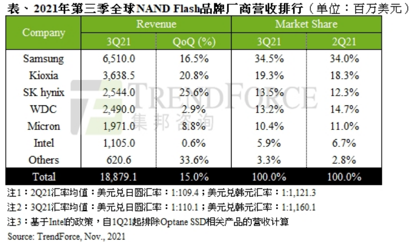
From the demand side, NAND Flash for smartphones and servers contributed most of the revenue in the third quarter. Q3 is the peak season for traditional smartphone shipments. Manufacturers such as Apple, OPPO, vivo, and Xiaomi have released flagship models to boost NAND Flash usage. On the other hand, the volume of ultra-large-scale data centers also drives NAND Flash revenue.
It seems that the global NAND Flash market is in great condition, but there are divergent opinions on the industry development trend in the fourth quarter and even 2022. TrendForce Consulting believes that due to the unresolved problem of insufficient upstream foundry capacity, the unbalanced supply of parts and components has extensively affected various applications, and the relatively sufficient inventory has led to a decline in contract prices. It is expected that the fourth quarter of this year NAND The momentum of Flash's strong revenue growth will temporarily come to an end.
Taiwan media also quoted industry sources as saying that since the fourth quarter of this year, the shortage of power management ICs and flash memory device controller chips has continued to improve, encouraging NAND flash memory chip manufacturers to expand production. The person also warned that the supply of NAND Flash may exceed demand in the first half of 2022.
Other opponents believe that the market is too pessimistic about the trend of NAND Flash. Pan Jiancheng, chairman of the NAND Flash control IC factory Phison, pointed out at the law conference that from the current point of view, the overall NAND Flash market capacity demand will grow by another 1.5 in 2022. ~1.8 times. It is expected that Phison's inventory will be insufficient to meet market demand in the first half of 2022 at the earliest. In the future, for emerging applications such as 5G and electric vehicles, the demand for NAND Flash capacity will not see the ceiling.
However, the cyclical demand for storage also determines the uncertainty of the NAND Flash market. The future trend remains to be further observed by the market.
Major players compete
When it comes to NAND Flash, we have to mention the most mainstream 3D NAND on the market. Related data shows that in 2019, the penetration rate of 3D NAND reached 72.6%, far exceeding 2D NAND. It is expected that this number will reach 97.5 in 2025. %.
From 2D to 3D has long been a major trend in the NAND Flash market. For this change, there is a vivid analogy that is "from square to high-rise."
So why did NAND Flash evolve into 3D? Jim Handy, chairman and senior analyst of Objective Analysis, an analyst firm, pointed out in the guest "Jiwei Interview" that "3D NAND is a way for NAND storage manufacturers to overcome current difficulties. They have no way to reduce costs on the basis of the original 2D NAND storage. , So they chose to use 3D technology to'throttle'."
More importantly, 3D NAND also solves the problem of 2D NAND's performance degradation while increasing capacity.
The advantages of this technology naturally attracted many players into the game. Samsung, Kioxia, SK Hynix, Micron, Yangtze River Storage and other manufacturers have deployed 3D NAND Flash.
From the perspective of technological development, each company is still competing in the number of layers. Samsung began mass production of 3D NAND Flash as early as 2013, using the CTF charge trap flash (CTF) route, which is less technically difficult than the traditional FG (Floating Gate). At present, Samsung has mass-produced 176-layer NAND Flash. In addition, Samsung also announced the details of the next-generation NAND Flash, with a stack of more than 200 layers.
SK Hynix, another major storage company in South Korea, announced a major event last year, namely the acquisition of Intel’s NAND Flash business for US$9 billion, and it has passed antitrust investigations in various countries. In terms of product development, it is reported that SK Hynix will begin mass production of 176-layer NAND Flash in the fourth quarter of this year.
Kioxia invested in research and development earlier. In 2007, it launched BiCS technology in a unique way. In February of this year, it announced the joint development of 162-layer NAND Flash with Western Digital.
Micron is the first manufacturer in the world to announce the mass production of 176-layer NAND Flash. This product combines a new array structure with a replacement gate process and a new cell structure to improve performance while reducing size.
Yangtze River Storage in Mainland China entered the market late. In 2017, it released its first 3D NAND Flash. In 2019, based on the self-developed Xtacking®1.0 architecture flash memory technology, it successfully mass-produced 64-layer TLC 3D NAND flash memory. This year, 128-layer 3D NAND Flash will be mass-produced.
Where is the future?
In fact, not only the number of layers, but also the production capacity. Samsung Electronics will install a new 3D NAND chip production line at the Pyeongtaek No. 3 Plant (P3) to increase the output of 176-layer 3D NAND chips. By then, it will have a monthly production capacity of 40,000 to 50,000; Kioxia and Western Digital plan this spring To build a 1 trillion yen ($9.45 billion) factory in Yokkaichi, Japan, and it is expected to open the first batch of production lines in 2022. At the same time, Kioxia has also acquired many factories next to the Kitakami factory in Japan so that it can expand production capacity as needed in the future. In addition, news of SK Hynix and Micron starting to increase the production of 176-layer 3D NAND chips from the fourth quarter continues.
Now that 176-layer 3D NAND Flash has been mass-produced, and 200-layer or higher-layer products have also been exposed, where will 3D NAND Flash go in the future?
SK Hynix shared its views at the IEEE International Reliability Physics Symposium in March this year. It believes that the number of layers of 3D NAND Flash can be expanded to more than 600 in the near future. By then, each layer will become Thinner, smaller NAND unit, larger storage capacity. Another industry expert pointed out that 3D NAND Flash can be stacked to 1000 layers.
However, the greater the number of layers, the greater the technical difficulty. Jim Handy explained that in order to reduce costs through a 3D structure, it is necessary to increase the stack layer by layer, and then drill holes through each layer to complete the entire process. How to ensure the accuracy of the drilling while drilling deeper, and avoid the direction deviation that causes the channel to narrow below or narrow at the top and wide at the bottom is the biggest problem facing 3D NAND. Therefore, major storage vendors have spent a lot of time and energy studying how to increase the number of layers while making each layer thinner.
It is understood that the current "secret" for storage vendors is to first stack 32 or 64 layers to drill holes, then stack 32 or 64 layers on top, and then drill holes. "This method is feasible, and this technology has not yet found a limit on the number of layers." Jim Handy added.
From the perspective of the development of each company, they are pursuing a higher number of layers to increase storage capacity. Kioxia CEO Liu Maozhi said at the flash memory summit, "Some people may think that the number of stacked layers is the most important parameter for the growth of 3D NAND capacity. , But it’s not completely correct. There is no need to increase the number of stacked layers at the expense of increased thickness."
Summary: Although it is still impossible to predict how many layers of 3D NAND Flash can be stacked, it can be expected that the number of layers and capacity wars of major global storage vendors such as Samsung, SK Hynix, Kioxia, Micron, and Yangtze River Storage will continue. .