DB HITEK будет использовать технологию нитрида на основе кремния для улучшения 8-дюймового полупроводникового процесса
Jan 05,2022
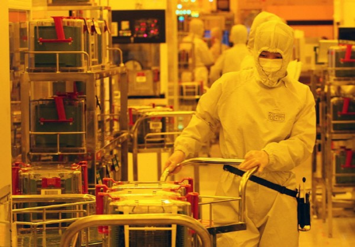
Южнокорейская литейная компания DB HITEK производит полупроводниковые чипы путем изготовления тонких пленок из материалов нитрида галлия (GAN) на кремниевых вафли. Эта технология может реагировать на быстрый рост оборудования связи, зарядных устройств электромобилей и солнечных конвертеров. Рынок.
Согласно корейским СМИ ETNEWS, GAN является полупроводниковым материалом следующего поколения, который может улучшить энергоэффективность оборудования связи, быстрых зарядных устройств для электромобилей и солнечных конвертеров. DB HITEK будет производить 8-дюймовые полупроводники, основанные на технологии GAN-on-Si, который, как ожидается, упростит обработку вафли для повышения прибыльности путем повышения конкурентоспособности производства полупроводниковых продуктов.
Понятно, что DB HITEK ожидает использовать его завод Чунгбука для решения 8-дюймового рынка в этом году. Компания планирует в полной мере использовать емкость Chungbuk Sangwoo Fab или внести дополнительные инвестиции для удовлетворения спроса на 8-дюймовые полупроводники, такие как электромобили и электрооборудование.